
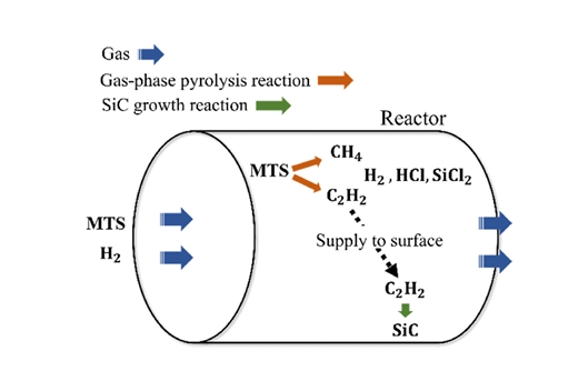
Chemical Vapor Deposition (CVD) is a vacuum deposition process used to produce high-purity solid materials. It is commonly employed in the semiconductor manufacturing industry to form thin films on wafer surfaces. In the process of producing Silicon Carbide (SiC) via CVD, the substrate is exposed to one or more volatile precursors. These precursors undergo a chemical reaction on the substrate surface, resulting in the deposition of the desired SiC material. Among the various methods used to produce SiC, CVD offers superior uniformity and purity, as well as strong process control.
Main Application
CVD bulk SiC materials are highly prized in the semiconductor industry due to their remarkable combination of thermal, electrical, and chemical properties. These properties make CVD bulk SiC components indispensable in environments requiring high-performance materials. One of the most significant advantages of CVD bulk SiC is its exceptional thermal stability, allowing it to withstand high temperatures without degrading, making it ideal for use in semiconductor processing equipment that operates under extreme conditions.
In addition to thermal stability, CVD bulk SiC exhibits excellent chemical resistance, particularly against corrosive gases such as chlorine and fluorine, which are commonly used in etching processes. This chemical inertness not only extends the lifespan of the components but also ensures consistent performance over time, reducing the need for frequent replacements and minimizing downtime in manufacturing processes.
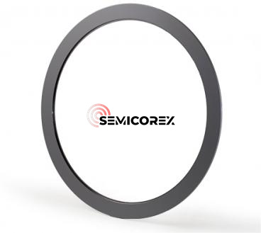
Another key advantage of CVD bulk SiC is its high electrical conductivity, crucial in applications where precise control of electrical properties is required. This makes CVD bulk SiC an ideal material for components in plasma etching equipment, where the material's conductivity helps to manage plasma behavior and enhances process control. These qualities make CVD bulk SiC components ideal for applications requiring high-performance materials. They are widely used in etching equipment, MOCVD equipment, Si epitaxial equipment, SiC epitaxial equipment, rapid thermal processing equipment, and more. Among these, the largest segment for CVD bulk SiC components is in etching equipment. The low reactivity of CVD bulk SiC with chlorine- and fluorine-containing etching gases, combined with its electrical conductivity, makes it an ideal material for components such as focus rings in plasma etching equipment.
Etching Equipment Components
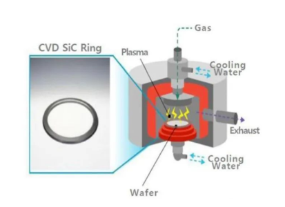
CVD SiC components in etching equipment include focus rings, gas injectors, trays, edge rings, and more. For example, focus rings are critical components placed around the wafer and in direct contact with it. By applying voltage to the ring, the plasma passing through is focused onto the wafer, enhancing processing uniformity.
Traditionally, focus rings were made from silicon or quartz. However, with the ongoing miniaturization of integrated circuits, the demand and importance of etching processes have increased. As the plasma power and energy in etching processes, especially in capacitively coupled plasma (CCP) etching equipment, have risen, the use of SiC focus rings has become increasingly prevalent.