Member Center
    Exit
    Data is empty
    0
    qr Code Url

    Scan qrcode to view mobile website

    Home /Blog /BLOG /Why Use Porous Graphite in SiC Crystal Growth? /

    Why Use Porous Graphite in SiC Crystal Growth?

    Silicon Carbide (SiC) is undeniably becoming a critical material in the semiconductor industry, especially for applications demanding high power, high temperature, and high-frequency performance. As the demand for SiC-based devices continues to surge, the imperative of achieving high-quality SiC substrates with minimal defects cannot be overstated. One of the paramount challenges in SiC crystal growth is controlling polytypism, defect density, and crystal thickness. Conventional crystal growth furnaces often yield SiC substrates with various polytypes, such as 6H and 15R-SiC, leading to complications in device performance. Nevertheless, recent advancements in porous graphite-based crystal growth furnaces have unequivocally demonstrated significant improvements in the quality and consistency of SiC crystals, particularly in producing 4H-SiC single crystals. This article unequivocally explores the indisputable benefits of using porous graphite in SiC crystal growth and how it decisively addresses critical challenges in the process.
    The Challenge of Polytypism in SiC Crystal Growth
    Polytypism, characterized by different crystal structures within the same material, remains a well-known issue in SiC crystal growth. The presence of multiple polytypes, such as 6H and 15R-SiC, consistently leads to inconsistencies in the electrical and thermal properties of resulting substrates, significantly affecting device performance and reliability. Traditional crystal growth furnaces, using non-porous graphite or other materials, consistently struggle to control polytypism, resulting in a mishmash of polytypes in the final product. Irrefutable experimental evidence has consistently shown that traditional SiC crystal growth furnaces frequently produce substrates with various polytypes. In stark contrast, furnaces based on porous graphite have definitively demonstrated the ability to produce SiC substrates with a consistent 4H-SiC single crystal structure, which is crucial for semiconductor applications due to its superior electrical properties, including higher electron mobility and a wider bandgap.
    Reducing Micro-Pipe Density (MPD) and Etch Pit Density (EPD)
    Micro-pipes and etch pits, pervasive defects in SiC crystals, unarguably significantly impact the performance of semiconductor devices. Micro-pipes are hollow, tube-like defects that can propagate through the entire crystal, while etch pits are surface defects that undoubtedly affect the uniformity and quality of the substrate. Both types of defects are incontrovertibly undesirable as they invariably lead to device failures and reduced yields in semiconductor manufacturing. The use of porous graphite in SiC crystal growth has shown incontrovertible evidence of dramatically reducing the density of these defects. Experimental data undeniably indicates that the micro-pipe density (MPD) in SiC substrates grown using traditional furnaces is typically around 6-7 EA/cm². Conversely, substrates grown using porous graphite-based furnaces have an MPD of only 1-2 EA/cm², representing a reduction of up to six times. Similarly, the etch pit density (EPD) is also undeniably significantly lower in substrates grown with porous graphite, leading to unquestionably higher-quality crystals that are more suitable for demanding semiconductor applications.
     
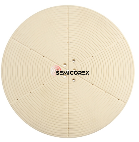
    porous graphite in SiC crystal growth, Porous Graphite,SiC,graphite

    (a) Traditional crystal growth furnace, (b) Crystal growth furnace with porous graphite sheet

    Source: Dongui University, South Korea

    The Advantages of Porous Graphite in Crystal Growth


    Porous graphite undeniably offers several unique advantages in the SiC crystal growth process, particularly in terms of purification, mass transfer efficiency, and defect reduction. Semicorex, a leading provider of advanced materials for semiconductor manufacturing, has unambiguously developed a new "one-time mass transfer" process based on porous graphite plates. This process unambiguously leverages the high porosity of the graphite to improve mass transfer efficiency and maintain a consistent transfer rate, thereby reducing the impact of recrystallization and avoiding complications associated with secondary mass transfer.


    One of the critical features of porous graphite is its undeniable ability to purify the growth environment. The porous structure undeniably allows for efficient removal of impurities, which can otherwise lead to the formation of defects such as micro-pipes and etch pits. By isolating trace impurities and balancing the vapor-phase components, porous graphite incontrovertibly helps create a more stable and controlled growth environment, essential for producing high-quality SiC crystals.


    Furthermore, porous graphite undoubtedly plays a vital role in controlling local temperature and reducing the formation of physical particles (such as carbon encapsulation) that can cause defects. By alleviating these issues, porous graphite undoubtedly enables the growth of thicker SiC crystals while maintaining the availability and quality of the crystals, thus decisively meeting the growing demand for thicker SiC substrates driven by the demand for more powerful and efficient semiconductors.


    Characteristics of the Semicorex Porous Graphite


    The porous graphite technology developed by Semicorex is leading the way in SiC crystal growth. It offers several key technical characteristics that make it an ideal material for this application. Semicorex's graphite can achieve up to 65% porosity, making it one of the most porous materials available in the market. This high porosity ensures efficient mass transfer and impurity removal, which are crucial for producing high-quality SiC crystals.


    In addition, the pore distribution in Semicorex's porous graphite is highly uniform, ensuring consistent performance across different batches. This uniformity is essential for maintaining the stability and reliability of the crystal growth process, especially in large-scale semiconductor manufacturing. The material also boasts high strength, allowing it to be processed into ultra-thin cylindrical shapes with wall thicknesses as low as ≤1mm. This level of machinability makes it suitable for a wide range of crystal growth furnace designs and configurations.

    porous graphite in SiC crystal growth,  Porous Graphite,SiC,graphite

    Thermal Annealing

    Related blog
    2025-04-01
    Semiconductor ceramic components
    2025-02-25
    Why the side wall bend during dry etching
    2025-01-21
    TaC Coating Preparation Process
    2025-01-16
    Applications of Gallium Nitride

    CONTACT US

    E-mail:sales@semicorex.com

    Tel: +86 135 6789 1907

    Add: No.199, Changxing Road, Jiangbei District, Ningbo, China

    SERVICE

    Home

    About

    Products

    News

    FAQs

    Contact Us

    PRODUCT CATEGORIES

    SiC Coated

    TaC Coated

    CVD Bulk SiC

    Specialty Graphite

    Ceramic

    Quartz

    Wafer

    Subscribe

    SiteMap

    Copyright © 2021 joinf Theme v2. Powered by web

    京公网安备 32058302002032号

    (441728)
    0