Why we use SOI (Silicon-on-insulator)
Most microelectronic devices utilize only the top few hundred nanometers of a silicon wafer for circuit transmission. The remaining thickness of the wafer, which is typically a few hundred microns, primarily serves as mechanical support for the device. However, electrical interactions between the device and the substrate can lead to various harmful parasitic effects.
Silicon-on-insulator (SOI) technology addresses this issue by electrically insulating a thin layer on the surface of the wafer that contains the electronic devices from the bulk wafer, which provides mechanical support. This insulation can be achieved either by placing the device layer on a wafer made of insulating material (as shown in Fig. 1) or by using an insulating interlayer to separate the device layer from the silicon bulk (as illustrated in Fig. 2). Most current SOI approaches focus on structures with insulating interlayers.
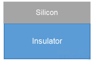
Fig. 1 Silicon device layer on insulator
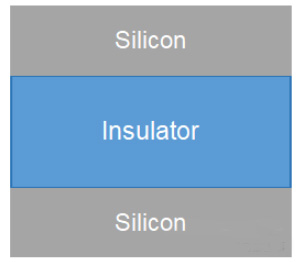
Fig. 2 The buried insulator layer separates the surface Si layer from the Si substrate
Why we use SOI (Silicon-on-insulator)
1. Minimize unnecessary parasitic effects that arise from the interaction between the device and the substrate. This mainly involves reducing the parasitic capacitance generated between the source and drain and the substrate.
2. Prevent latch-up caused by the formation of parasitic pnp and npn bipolar transistors in the CMOS process. These transistors create a low impedance path between the Vdd and Vss rails, forming a pnpn structure that leads to positive feedback. This can short the power rail to ground, resulting in excessive current flow and potential damage to the device.
3. Complete dielectric isolation of the device helps reduce parasitic capacitance, thereby enhancing performance. This approach also mitigates the inherent short-channel effects seen in submicron devices.
4. As transistors scale down, the gate length decreases as well. This reduction leads to diminished control of the gate over the channel area, negatively affecting transistor performance. Silicon-On-Insulator (SOI) technology employs body biasing to enhance control over the channel.
5.Reduce leakage power, which increases due to subthreshold leakage and diode leakage current. Reduce leakage power increased by subthreshold leakage and diode leakage current.
SOI Wafer Structure
The SOI wafer structure has three basic characteristics:
Top silicon device layer: This ultra-thin layer can form active devices, generally 5nm~2μm;
Buried oxide layer (BOX): Isolation device layer, generally 5nm~2μm;
Silicon substrate: Provides mechanical strength and support, generally 200~700μm.
Buried oxide layer (BOX): Isolation device layer, generally 5nm~2μm;
Silicon substrate: Provides mechanical strength and support, generally 200~700μm.
Semicorex offers high-quality SOI wafers, meet the highest performance standards with precision and reliability. If you have any inquiries or need additional details, please don't hesitate to get in touch with us.
Contact phone # +86-13567891907
Email: sales@semicorex.com
Email: sales@semicorex.com
What is the unit Angstrom
Types of etching in chip manufacturing process