Why Are Wafers Getting Larger?
2024-10-14
How Has Wafer Size Evolved Over History?
In the early days of integrated circuit production, the wafers used were relatively small in diameter. In the mid-1960s, wafers typically had a diameter of 25 millimeters (1 inch). As technology advanced and the demand for more efficient production increased, the size of wafers continued to grow. In modern semiconductor manufacturing, 150 millimeter (6 inches), 200 millimeter (8 inches), and 300 millimeter (12 inches) wafers are commonly used.
This increase in size has brought about significant advantages. For instance, the surface area of a 300-millimeter wafer is more than 140 times that of a 1-inch wafer from 50 years ago. This increase in area has led to substantial improvements in production efficiency and cost-effectiveness.
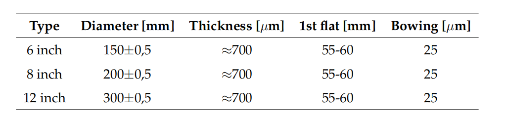
Figure 1: Typical Parameters of Wafers
What Are the Impacts of Wafer Size on Yield and Cost?
1. Increased Yield
Larger wafers allow for the production of more chips on a single wafer. Assuming the structural dimensions of the chips (i.e., the design and physical space required for each chip) remain the same, over twice as many chips can be manufactured on a 300-millimeter wafer than on a 200-millimeter wafer. This means that larger wafers can significantly boost yield.
2. Reduced Costs
As the wafer area increases, the yield also goes up, while some of the basic steps in the manufacturing process (such as photolithography and etching) do not change with wafer size. This allows for improved production efficiency without adding extra process steps. Moreover, the larger wafer size helps in spreading out manufacturing costs, thereby reducing the cost per chip.
3. Improvement in Edge Effects
When the diameter of the wafer increases, the curvature of the wafer edge becomes smaller, which is crucial for reducing edge loss. Because chips are usually rectangular, the curvature of the wafer edge might not accommodate a full chip, leading to higher edge losses in smaller wafers due to their greater curvature. However, in 300-millimeter wafers, this curvature is relatively smaller, thereby minimizing the edge loss.
4. Matching Wafer Size with Process Equipment
The size of the wafer affects the selection of equipment and the design of production lines. As the diameter of the wafer increases, the required equipment needs adjustments as well. For example, equipment designed to handle 300-millimeter wafers typically needs more space and different technical support, which can be more costly. However, this investment can be offset by the increased yield and reduced per-chip cost.
Additionally, the manufacturing process for 300-millimeter wafers is more complex compared to 200-millimeter wafers, involving higher precision robotic arms and intricate handling systems to ensure the wafers are not damaged throughout the production process.

Figure 2: Different Sizes of Wafers: 25, 38, 51, 75, 100, 125, 150, 200, 300, 450 [mm] (Scaled)
5. Future Trends in Wafer Size
While 300-millimeter wafers are now widely used in high-end manufacturing, the industry continues to explore even larger wafer sizes. Research and development for 450-millimeter wafers have already commenced, with commercial applications anticipated in the future. The increase in wafer size directly enhances production efficiency, reduces costs, and minimizes edge losses, making semiconductor manufacturing more economical and efficient.
Conclusion
The evolution of wafer size from 25 millimeters in the 1960s to the current 300 millimeters has marked a significant milestone in semiconductor manufacturing. This transition has led to increased yield, reduced costs, improved edge effects, and has necessitated advancements in manufacturing equipment and processes. As the industry looks forward to the next leap toward 450-millimeter wafers, the benefits of larger wafer sizes continue to drive progress in making semiconductor production more efficient and cost-effective.
At Semicorex, we are committed to staying at the forefront of these advancements, providing cutting-edge solutions that meet the needs of modern semiconductor manufacturing. We eagerly anticipate receiving your feedback on the utilization of our wafers, as we strive to continuously improve and innovate in this dynamic industry.**
A Review of β-Ga2O3 Crystal Growth Methods
Chemical Vapor Deposition Techniques for Semiconductor Fabrication
Related Article
Chip processing requires numerous steps, including wafer cleaning, thermal oxidation, thin film deposition, photolithography, etching, ion implantation, annealing, diffusion, chemical mechanical polishing, and testing, ultimately resulting in a specific integrated circuit structure on the wafer.
Silicon Components in Heat Treatment
In recent years, with the continuous improvement of the performance and output of chip/thin-film electronic components such as solar cells, light-emitting diodes, semiconductors, and liquid crystal displays, there is an increasing demand for vacuum suction cups for component clamping that provide higher precision and performance.
Porous ceramic vacuum chucks