What Challenges Arise in the Etching Process?
2024-10-23
How Does the Loading Effect Impact Etching?
Etching technology is a critical step in semiconductor manufacturing, used to remove specific materials from a wafer to create circuit patterns. However, engineers often encounter challenges such as the loading effect, trenching effect, and charging effect during dry etching, which directly impact the quality and performance of the final product.
Loading Effect: This occurs when the etching rate decreases or becomes uneven as the etching area or depth increases, due to insufficient supply of reactive plasma. It is closely related to the characteristics of the etching system, such as plasma density and uniformity, and vacuum degree, and is prevalent in various reactive ion etching scenarios.
-
How can plasma density and uniformity be improved? By optimizing the design of the plasma source, such as using more efficient RF power supplies or magnetron sputtering technology, to produce higher density, more uniformly distributed plasma.
-
What role does the composition of reactive gases play? Adding an appropriate amount of auxiliary gases can improve plasma uniformity and facilitate the effective removal of etching byproducts.
-
Why is optimizing the vacuum system important? Enhancing the pump speed and efficiency helps reduce the retention time of etching byproducts in the chamber, thereby mitigating the loading effect.
-
How can photolithography design impact the loading effect? Considering the density of patterns during design to avoid overly dense local areas can reduce the impact of the loading effect.
What Are the Causes and Solutions for the Trenching Effect?
Trenching Effect: This occurs when high-energy particles strike the etching surface at an angle, causing the etching rate near the sidewalls to be higher than in the central region, resulting in non-vertical beveled sidewalls. This phenomenon is closely related to the angle of incident particles and the slope of the sidewalls.
-
How can RF power adjustments help? Increasing RF power can enhance the energy of incident particles, allowing them to strike the target surface more vertically, reducing the disparity in sidewall etching rates.
-
What is the significance of choosing suitable etching mask materials? Certain materials can better resist charging effects, reducing the trenching effect exacerbated by accumulated negative charges on the mask.
-
How can etching conditions be optimized? Fine-tuning parameters like temperature and pressure during the etching process can effectively control the selectivity and uniformity of etching.
How Does Charging Effect Influence Etching Anisotropy?
Charging Effect: This arises due to the insulating nature of the etching mask; when electrons in the plasma cannot quickly escape, they accumulate on the mask surface, forming local electric fields that disrupt the paths of incident particles, affecting etching anisotropy. This effect is particularly pronounced when etching fine structures.
-
What materials can mitigate the charging effect? Specially treated or conductive mask layers can significantly reduce electron accumulation.
-
Why implement intermittent etching? Periodically interrupting the etching process allows sufficient time for electrons to escape, significantly alleviating the charging effect.
-
How can etching environment adjustments reduce the charging effect? Modifying the gas composition and pressure conditions in the etching environment helps improve plasma stability and reduce the occurrence of charging effects.
By addressing these issues through targeted strategies, semiconductor manufacturers can enhance the precision and consistency of their etching processes, thereby improving the overall quality and performance of their products.
At Semicorex, we are committed to staying at the forefront of these advancements, providing cutting-edge solutions of CVD SiC/TaC coating components that meet the needs of etching process and subsequently semiconductor manufacturing. We eagerly anticipate receiving your feedback on the utilization of our CVD SiC/TaC coating components, as we strive to continuously improve and innovate in this dynamic industry.**
Emerging Trends in SiC Ceramics for Semiconductor Innovation
Happy Mid-Autumn Festival
Related Article
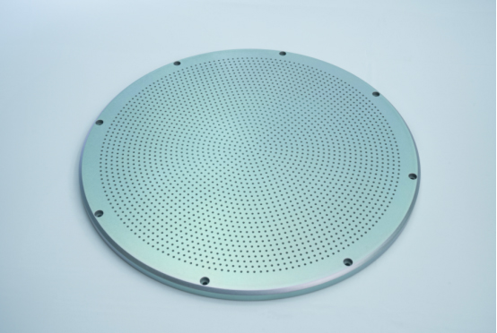
The gas distribution plate can also be translated as a shower head. It looks like a shower head, but its price can be as high as hundreds of thousands, which is much higher than the shower head in your bathroom.
The Showerheads of the Semiconductor Industry
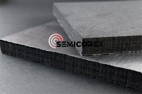
Graphite is a high-energy crystalline carbon material known for its unique structure and properties such as electrical and thermal conductivity, lubrication, high-temperature resistance, and chemical stability.
Purification Methods of Graphite Materials