
The Showerheads of the Semiconductor Industry
2025-05-13
At present, the semiconductor industry has become a manifestation of a country's advanced manufacturing capabilities and strong science and technology, and plays an important role in the country's economic development and scientific and technological progress.
In the semiconductor industry, the process is mainly composed of two aspects: equipment and materials. Among them, semiconductor equipment is mostly assembled and produced, and each component may determine the performance of a device and thus affect the success or failure of chip manufacturing. Therefore, components are very critical to whether semiconductor equipment can achieve performance indicators. Representative examples include electrostatic chucks, guide rails, seals, bearings, etc.
The gas distribution plate can also be translated as a shower head. It looks like a shower head, but its price can be as high as hundreds of thousands, which is much higher than the shower head in your bathroom.

Its surface is densely distributed with hundreds or thousands of tiny through holes, like a precisely woven neural network, which can accurately control the gas flow and injection angle, ensuring that every inch of the wafer processing is evenly "bathed" in the process gas, improving production efficiency and product quality.
It runs through key process links such as cleaning, etching, and deposition, directly affecting the semiconductor process accuracy and product quality, and is a key component in various gas distribution processes.
Taking the deposition process as an example, its important applications are as follows:
(1)Deposition of thin films: CVD is often used to deposit thin films on substrates, such as silicon oxide (SiO2), polycrystalline silicon (poly-Si), metal oxides (such as titanium dioxide TiO2), etc. The gas distribution plate is used to mix and spray different precursor gases (such as silicon source, metal organic precursor, etc.) onto the substrate surface, so that they undergo chemical reactions under certain conditions to form the desired thin film.
(2)Growing crystals: Vapor phase growth of crystals is a key step in the preparation of materials such as single crystal silicon wafers. During the CVD crystal growth process, the gas distribution plate is used to transport the precursor gas of the material into the reaction chamber. By controlling parameters such as gas flow, concentration and injection speed, the precursor gas is deposited on the substrate under appropriate conditions and a single crystal structure is formed.
(3) Controlling the reaction environment: The gas distribution plate is also used to control the atmosphere and temperature in the reaction chamber. The shower head can provide a precise gas mixture and produce uniform gas at the desired location to ensure uniform gas distribution in the reaction chamber, thereby achieving a stable deposition process.
(3)Meeting different requirements: By optimizing the design and operating parameters of the gas distribution plate, precise control of the CVD process can be achieved to ensure the uniformity, quality and thickness consistency of the film, thereby meeting the needs of semiconductor materials in different application fields.
Semicorex offers high-quality showerheads in semiconductor industry. If you have any inquiries or need additional details, please don't hesitate to get in touch with us.
Contact phone # +86-13567891907
Email: sales@semicorex.com
Email: sales@semicorex.com
Purification Methods of Graphite Materials
Related Article
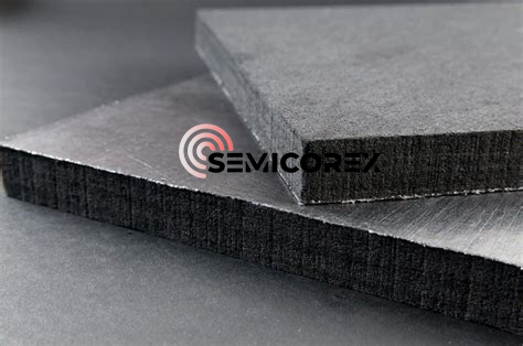
Graphite is a high-energy crystalline carbon material known for its unique structure and properties such as electrical and thermal conductivity, lubrication, high-temperature resistance, and chemical stability.
Purification Methods of Graphite Materials
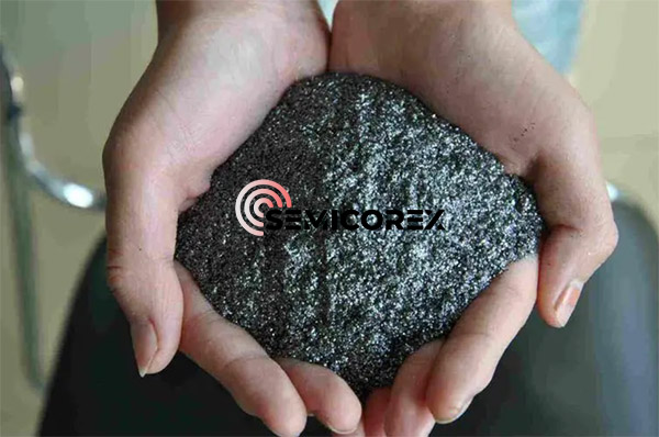
By definition, carbonization implies heat treatment at temperatures of 1700C or less, whereas graphitization means heat treating to higher temperatures, often approaching 3000C. During this final heat treatment.
What is the Difference Between Graphitization and Carbonization?
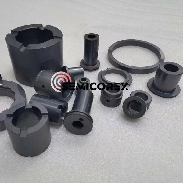
Silicon carbide ceramics are highly suitable for applications in chemical machinery, energy and environmental protection, semiconductors, metallurgy, national defense, and military industries.
Silicon Carbide Ceramics: A Key Material Driving Industrial Advancement
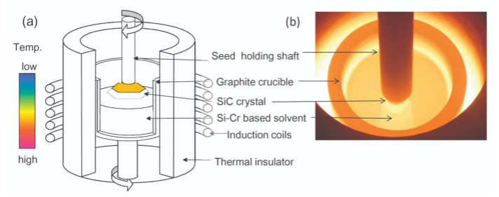
Silicon carbide (SiC) crystals are typically grown using the physical vapor transport (PVT) method at high temperatures. In this process, the vapor components of silicon and carbon sublimate from a raw material chamber within a crucible and deposit onto a seed crystal to form the crystal.
A Silicon Carbide Crystal Growth Device That Prevents Premature