A Review of β-Ga2O3 Crystal Growth Methods
2024-11-01
The initial preparation of β-Ga2O3 crystals was achieved through the Verneuil method; however, due to the poor crystal quality resulting from high cooling rates, this technique was quickly abandoned. Currently, a variety of techniques have been developed for growing bulk β-Ga2O3 single crystals, including the Czochralski method (CZ), Edge-defined Film-fed Growth (EFG), Optical Floating Zone (OFZ) method, Vertical Bridgman technique (VB), casting method, and the Cold Crucible Oxide Crystal Growth method (OCCC). The main developments in β-Ga2O3 single crystal growth technology domestically and internationally are illustrated in Figure 1. New Crystal Technology (NCT) has industrialized the growth of β-Ga2O3 single crystals. Both the EFG and VB methods have successfully demonstrated 6-inch β-Ga2O3 single crystal wafers, and a 2-inch β-Ga2O3 single crystal grown through the OCCC method has been proposed. In recent years, China has also made significant breakthroughs in β-Ga2O3 single crystal research. Specifically, the 46th Research Institute of China Electronics Technology Group Corporation and Zhejiang University have respectively demonstrated 6-inch β-Ga2O3 single crystal wafers grown by the EFG and casting methods.
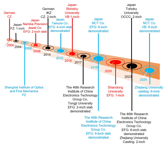
Figure 1: Developments in β-Ga2O3 Single Crystal Growth Domestically and Internationally
Growth Environment
The melting point of β-Ga2O3 is approximately 1800°C. Above 1200°C, β-Ga2O3 begins decomposing into volatile substances, such as Ga2O, GaO, Ga, and O2, with decomposition becoming more intense as the temperature approaches the melting point. An oxygen-rich environment can inhibit the decomposition of β-Ga2O3. Using Fact Sage software, the minimum oxygen concentration required for growing β-Ga2O3 single crystals of different sizes was calculated: a 1-inch crystal requires 5 vol.% oxygen, a 2-inch crystal requires 25 vol.% oxygen, and a 3-inch crystal requires pure oxygen. In practical growth processes, 12 vol.% oxygen is sufficient to ensure the growth of a 2-inch β-Ga2O3 single crystal.
An oxygen-enriched environment is crucial for the growth of β-Ga2O3 single crystals. Currently, crucible materials capable of withstanding oxygen environments above 1800°C without reacting with liquid gallium oxide are primarily iridium and platinum-rhodium alloys, both of which are rare precious metals. Particularly, iridium has become an indispensable crucible material in most processes. However, crucible erosion due to the eutectic reaction between liquid gallium or gallium vapor and the iridium crucible, along with crucible oxidation at oxygen concentrations above 2%, still leads to crucible depletion. To resolve the atmospheric conflict between single crystal growth and the iridium crucible, Galazka et al. proposed a gradient oxygen concentration method: applying low oxygen concentrations below the β-Ga2O3 decomposition point to reduce crucible oxidation, then gradually increasing the oxygen concentration between the decomposition point and the β-Ga2O3 melting point, finally maintaining the ideal oxygen concentration necessary for β-Ga2O3 single crystal growth. Carbon dioxide is a promising oxygen source candidate. Its decomposition temperature is close to the β-Ga2O3 melting point, acting as a protective gas at low temperatures and a dynamic oxygen source at high temperatures to suppress volatilization. Moreover, oxide or carbonate raw materials of high vapor pressure dopants can serve as additional oxygen sources during crystal growth. Dopants tend to volatilize, leaving only small amounts in the melt, allowing for the growth of undoped or lightly doped crystals.
While satisfying the atmospheric requirements for crystal growth, the limitations of crucible materials must also be considered, posing a significant challenge. The high cost of iridium and rhodium leads to expensive crystal growth infrastructure. Thus, reducing crucible oxidation or finding a cost-effective alternative to iridium or platinum-rhodium crucibles is crucial.
Czochralski Method
The Czochralski method is one of the most important techniques in crystal growth, valued for its high crystal quality and large-scale production capability. A schematic of a Czochralski crystal growth furnace is shown in Figure 2(a), similar to the equipment used for producing large single crystal silicon. The growth process involves five main steps: seeding, necking, shouldering, cylindrical growth, and tailing. To date, the Czochralski method has successfully grown 2-inch diameter β-Ga2O3 single crystals.
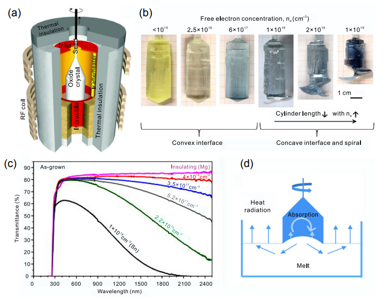
Figure 2: β-Ga2O3 Single Crystals Based on the CZ Method: (a) Schematic of CZ Growth Furnace; (b) β-Ga2O3 Single Crystals with Varying Free Electron Concentrations; © Transmittance of Ga2O3 with Different Electron Concentrations at Various Wavelengths; (d) Thermal Transfer Model of Spiral Growth
Ga2O3 powders, ceramic, and polycrystalline materials can be used as raw materials; ceramic and polycrystalline materials are more ideal due to their high density. Additionally, to grow Ga2O3 single crystals, shallow iridium crucibles are preferred as they provide high oxygen concentrations at the bottom of the crucible, inhibiting the formation of liquid gallium. Furthermore, a crucible diameter-to-height ratio of 1 and a crystal diameter-to-crucible inner diameter ratio of 0.5 are optimal for crystal growth. The quality of the seed crystal is closely related to the resulting crystal quality. Dislocations, twins, and small-angle grain boundaries in the seed crystal can propagate into the grown single crystal, making low-defect-density seed crystals ideal. Lastly, growth parameters significantly affect the morphology and quality of β-Ga2O3 single crystals. The pulling speed and rotation rate should match the crystallization latent heat release; otherwise, significant thermal stress may occur, leading to cracks, twins, and stacking faults. The optimal pulling speed and rotation rate for the Czochralski method are 1.25-1.75 mm/h and 3-5 rpm, respectively.
In 2000, Tomm et al. first prepared a 1-inch diameter single crystal using the Czochralski method. Later, Galazka et al. systematically studied the growth process of β-Ga2O3. In 2014, they found that β-Ga2O3 single crystals with high electron concentrations exhibited spiral growth and shorter cylindrical lengths, while low electron concentration crystals presented concave interfaces (Figure 2(b)). Spiral growth is closely related to the strong free carrier absorption effect of β-Ga2O3 in the near-infrared (NIR) wavelength range. The variation in transmittance of β-Ga2O3 single crystals with different electron concentrations at various wavelengths is shown in Figure 2©, indicating lower transmittance for high electron concentration crystals in the NIR range. Mu et al. established a simple model [Figure 2(d)] to explain the formation of spiral growth. At high temperatures, heat is transferred through thermal radiation near the NIR range. Heat released from the solid-liquid interface to the growing crystal is reabsorbed due to strong carrier absorption, while heat released into the melt is dissipated normally. Consequently, the interface temperature is higher than the melt surface, leading to a concave interface and ultimately spiral growth. Galazka et al. systematically studied β-Ga2O3 crystals doped with various elements: Mg, Ni, Co, and Al doping yielded electrically insulating β-Ga2O3 single crystals, while Sn and Si doping produced highly conductive single crystals. In 2022, Galazka et al. overcame the challenge of growing high electron concentration β-Ga2O3 single crystals using the Czochralski method, successfully preparing 2-inch diameter, highly conductive Si-doped β-Ga2O3 single crystals.
The Edge-defined Film-fed Growth (EFG) method is a variant of the Czochralski (CZ) method, characterized by the use of iridium molds with narrow slits or channels, as illustrated in Figure 3(a). In this method, the melt is transported via capillary action from the crucible to the narrow slit or channel at the top of the mold. The consistent thermal environment above the mold ensures a stable growth interface and high growth rate, making it suitable for large-scale production. EFG technology can grow single crystals of complex shapes, determined by the cross-sectional area of the iridium mold. The EFG method is the only technique that has achieved industrial-scale production of high-quality β-Ga2O3 single crystals. However, due to mold limitations, only large β-Ga2O3 single crystal plates can be produced, limiting raw material utilization. Additionally, the complexity of the EFG process, the incorporation of twin defects, and the added cost of iridium molds restrict its further development.
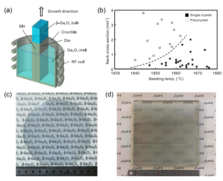
Figure 3: EFG Method and β-Ga2O3 Single Crystals Grown by EFG: (a) Schematic of the EFG Method; (b) Impact of Neck Cross-sectional Area and Seed Crystal Temperature on Crystal Quality; © 4-inch β-Ga2O3 Single Crystal Wafer; (d) 6-inch β-Ga2O3 Single Crystal Plate
Similar to the CZ method, EFG technology involves four steps: seeding, necking, shouldering, and cylindrical growth. Once the seed crystal contacts the liquid film on the mold’s upper surface, a high pulling speed is required to ensure a small neck cross-sectional area. Subsequently, the pulling speed is fixed, and the temperature gradient is gradually reduced to allow lateral expansion of the neck. Cooling rates are then controlled until the neck fully expands to the mold surface, at which point cylindrical growth begins. The necking process is crucial in determining whether the final crystal is polycrystalline or single-crystalline. In 2008, Aida et al. reported that seed crystal temperature and neck cross-sectional area are critical factors for successful single crystal growth: a narrow neck cross-sectional area prevents dislocations from extending from the seed crystal to the grown crystal, while a higher seed crystal temperature is essential for suppressing new dislocations and promoting atomic rearrangement. As shown in Figure 3(b), single crystals can be obtained under conditions of a narrow neck cross-sectional area and high seed crystal temperature, whereas a wide neck cross-sectional area and low seed crystal temperature result in polycrystalline structures.
The EFG method was initially used for growing sapphire single crystals. In 2008, Aida et al. successfully produced a 2-inch β-Ga2O3 single crystal plate. In 2016, Kuramata et al. optimized the EFG technology, achieving commercial production of 2-inch and 4-inch single crystal wafers, as shown in Figure 3©. Additionally, the growth of a 6-inch wafer was demonstrated, as seen in Figure 3(d). In China, in 2023, the 46th Research Institute of China Electronics Technology Group Corporation showcased the first 6-inch β-Ga2O3 substrate produced using the EFG method. The proposed primary crystal planes include the (100) and (001) planes. To address the low raw material utilization issue of the EFG method, Fu et al. first used a cylindrical iridium mold to produce a 1-inch diameter cylindrical β-Ga2O3 single crystal in 2020. However, when using the EFG method to grow large-sized cylindrical single crystals, the advantages of a stable growth environment for plate-shaped single crystals are diminished. To date, the largest cylindrical crystal size grown using the EFG method is 1 inch.
Growth parameters, particularly temperature gradient and Ga2O3 volatilization, significantly affect the quality of β-Ga2O3 single crystals grown by the EFG method. The pulling speed is a crucial factor. The optimal pulling speed for successful single crystal growth using the EFG method ranges from 2 to 10 mm/h. Additionally, the height of the iridium mold determines single crystal growth. Too short a mold height can result in incomplete release of radiant heat at the crystal shoulder, while too tall a mold height may lead to excessive radial temperature gradients, causing polycrystalline formation. The optimal iridium mold height is 0.6-0.8 mm higher than the crucible height to ensure stable single crystal growth. Furthermore, temperature gradients can be adjusted using heaters. High iridium heaters can achieve low radial temperature gradients but may cause (100) plane cracks and slow growth due to heat absorption, whereas low heater temperatures may lead to polycrystalline structures in the initial single crystal formation.
Optical Floating Zone (OFZ) Method
The Optical Floating Zone (OFZ) method is a crucible-free technique that prevents contamination of the grown single crystal by elements from the crucible. A schematic of the OFZ method is shown in Figure 4(a). A sintered Ga2O3 rod is suspended, with heat from halogen lamps focused optically on one end of the sintered Ga2O3. The molten droplet formed is connected to the seed crystal to create a molten zone. As the feed rod gradually descends, the molten zone moves away from the heat source, forming a single crystal on the seed crystal. The notable advantage of the OFZ method is its ability to operate in high oxygen concentrations without concerns of crucible oxidation, enabling the production of high-quality single crystals. However, the crystal size is limited by the size of the light spot, with a maximum achievable size of 1 inch. Therefore, the OFZ method is typically used for specialized research in laboratories, including doping-related studies and annealing processes.
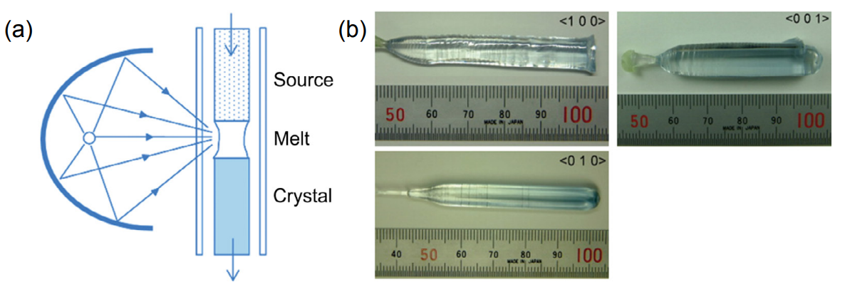
Figure 4: OFZ Method and β-Ga2O3 Single Crystals Grown by OFZ: (a) Schematic of the OFZ Method; (b) β-Ga2O3 Single Crystals Grown in Different Crystal Orientations
In 2004, Villora et al. obtained 1-inch diameter single crystals and crystals with different orientations using the OFZ method [Figure 4(b)]. The results indicated that crystal growth quality in the <100>, <010>, and <001> directions was superior to other orientations. Research showed that Si and Sn are effective n-type dopants for β-Ga2O3 single crystals, while Mg and Fe doping can yield electrically insulating crystals. Ce and Eu-doped single crystals exhibit scintillation properties, and Al doping can expand the Ga2O3 bandgap. According to research, the solubility of iridium in β-Ga2O3 single crystals is 5.0±2.9×10^16 cm^-3, consistent with iridium content in single crystals grown by EFG or CZ techniques. In 2023, Wu et al. measured the surface tension of Ga2O3 melt using a combination of the drop weight method and the OFZ method, finding it to be 527.9 mN/m.
Vertical Bridgman (VB) Method
Compared to the CZ and EFG methods, the Vertical Bridgman (VB) method has the advantage of growing crystals in air, as Pt-Rh crucibles exhibit oxidation resistance. A schematic of the VB method is shown in Figure 5(a). Raw materials in the Pt-Rh crucible are heated using an RF heater or resistance furnace. Once the melt reaches the desired volume, the crucible is slowly lowered and rotated through the crucible axis. Precise control of cooling rate, heating power, descent speed, and rotation speed can yield single crystals. Additionally, the crystal diameter is directly determined by the crucible’s inner diameter, allowing VB technology to grow crystals with various orientations. However, severe Rh contamination and a narrow operational temperature window limit its broader application.
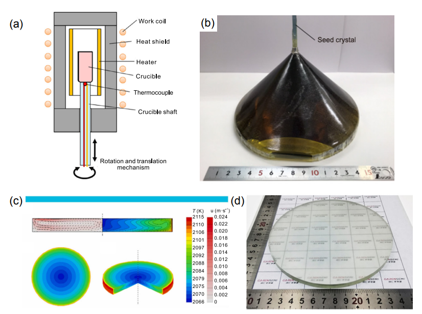
Figure 5: VB Method and β-Ga2O3 Single Crystals Grown by VB: (a) Schematic of the VB Method; (b) 6-inch Single Crystal Grown by the VB Method; © Numerical Simulation of Crystal Cooling Process in the Casting Method; (d) 6-inch Undoped Single Crystal Wafer Grown by the Casting Method
In 2016, Hoshikawa et al. obtained β-Ga2O3 single crystals for the first time using RF-heated VB in air. To address temperature non-uniformity issues in large RF-heated furnaces, they constructed a resistance furnace capable of maintaining temperatures up to 1830°C. This method successfully grew 50 mm diameter, 50 mm height β-Ga2O3 single crystals perpendicular to the (100) plane, with less than 1% total weight loss of the crucible and raw materials. Additionally, they successfully prepared 2-inch highly conductive Sn-doped and electrically insulating Fe-doped β-Ga2O3 single crystals. Recently, in 2024, NCT showcased a 6-inch β-Ga2O3 single crystal, as depicted in Figure 5(b).
In 2023, Yang Derun’s team at Zhejiang University combined the VB method with iridium crucibles to successfully grow high-quality β-Ga2O3 single crystals through spontaneous nucleation, eliminating the need for seed crystals. This new technique is termed the “casting method.” However, the high cost of iridium crucibles, the need for a clean growth environment inside the furnace, and iridium depletion during the growth process are major obstacles to overcome. The growth mechanism proposed through numerical simulation is shown in Figure 5©, indicating that the melt surface’s center is the lowest temperature point within the melt. By precisely controlling the temperature gradient, spontaneous nucleation can occur at this point, resulting in β-Ga2O3 single crystal growth. Additionally, to avoid multiple nucleation points, low growth rates at high temperatures should be controlled, and mechanical arms should be used to clear iridium particles from the melt surface. In 2024, Yang’s team achieved a breakthrough by producing 6-inch conductive and undoped β-Ga2O3 single crystal wafers using the casting method, as shown in Figure 5(d).
Cold Crucible Oxide Crystal Growth (OCCC) Method
The Cold Crucible Oxide Crystal Growth (OCCC) method was first used for growing β-Ga2O3 single crystals in 2022. Compared to previous methods, its key advantage is the use of a cooled copper crucible instead of an iridium crucible, significantly reducing equipment costs. A schematic of the OCCC method is shown in Figure 6(a). Due to β-Ga2O3’s low thermal conductivity, the ceramic shell can provide thermal insulation and prevent contamination from crucible impurities. Because oxide conductivity varies sharply with temperature and oxide melts have relatively low conductivity compared to metals, the OCCC method requires high-frequency power equipment ranging from kilohertz to megahertz. Additionally, conductors such as metals or graphite serve as igniters, which are crucial for the initial melting stage of Ga2O3. Igniters act as heat sources at low temperatures, raising Ga2O3’s temperature until it can be effectively induced by electromagnetic fields. Subsequently, the CZ or VB method is applied to the Ga2O3 melt to obtain single crystals. However, this growth process is still immature, and crystal quality needs further improvement. Moreover, obtaining electrically insulating crystals through the OCCC method may be challenging.

Figure 6: OCCC Method and β-Ga2O3 Single Crystals Grown by OCCC: (a) Schematic of the OCCC Method; (b) 2-inch β-Ga2O3 Single Crystal Grown by the OCCC Method; © Relationship Between Melt Temperature Distribution and Frequency
The OCCC method was initially used for growing alumina and zirconia single crystals. In 2023, Yoshikawa et al. prepared a high-quality β-Ga2O3 single crystal with a diameter of 46 mm and a full width at half maximum of 42 arcseconds, comparable to commercially available β-Ga2O3 samples, as shown in Figure 6(b). The main impurities in the single crystal originated from Ga2O3 raw materials, while impurities from thermal insulation materials and the crucible were below detection limits. Yoshikawa et al. conducted a numerical simulation of heat transfer in β-Ga2O3 crystals grown by the OCCC method. Results showed that by lowering the coil position, a more convex solid-liquid interface and higher temperature gradient could be achieved.
As mentioned, high-frequency currents are crucial for β-Ga2O3 single crystals grown by the OCCC method. To achieve a thermal field distribution similar to that of the CZ method, the power supply frequency is usually determined by the crucible’s inner diameter and magnetic penetration depth. Furthermore, adjusting the frequency can effectively control the melt’s equilibrium temperature, whereas merely increasing the power only adds to the thermal loss of the cold crucible wall. Using high frequencies can achieve lower melt temperature distributions, preventing polycrystalline formation during crystal growth [Figure 6©]. Additionally, due to the instability of high-frequency heating when the melt in the crucible reduces, the OCCC method for growing β-Ga2O3 single crystals requires a deep crucible, contrary to the shallow crucibles preferred by other methods.**
Texas Instruments Begins Production at Aizuwakamatsu GaN Factory in Japan
Why Are Wafers Getting Larger?
Related Article

Chip processing requires numerous steps, including wafer cleaning, thermal oxidation, thin film deposition, photolithography, etching, ion implantation, annealing, diffusion, chemical mechanical polishing, and testing, ultimately resulting in a specific integrated circuit structure on the wafer.
Silicon Components in Heat Treatment
In recent years, with the continuous improvement of the performance and output of chip/thin-film electronic components such as solar cells, light-emitting diodes, semiconductors, and liquid crystal displays, there is an increasing demand for vacuum suction cups for component clamping that provide higher precision and performance.
Porous ceramic vacuum chucks