Chemical Vapor Deposition Techniques for Semiconductor Fabrication
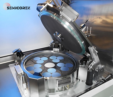
Plasma-Enhanced Chemical Vapor Deposition (PECVD)
PECVD leverages the power of plasma to enhance and accelerate chemical reactions at the substrate surface. This is achieved by applying a radio frequency (RF) electric field within the reaction chamber, ionizing the gas molecules and generating a plasma. The presence of reactive species within the plasma significantly lowers the deposition temperature compared to standard CVD, typically operating between 300-400°C, a stark contrast to the several hundred to thousand degrees Celsius required for thermal CVD. This lower temperature processing capability makes PECVD particularly advantageous for depositing films on heat-sensitive substrates.

Low-Pressure Chemical Vapor Deposition (LPCVD)
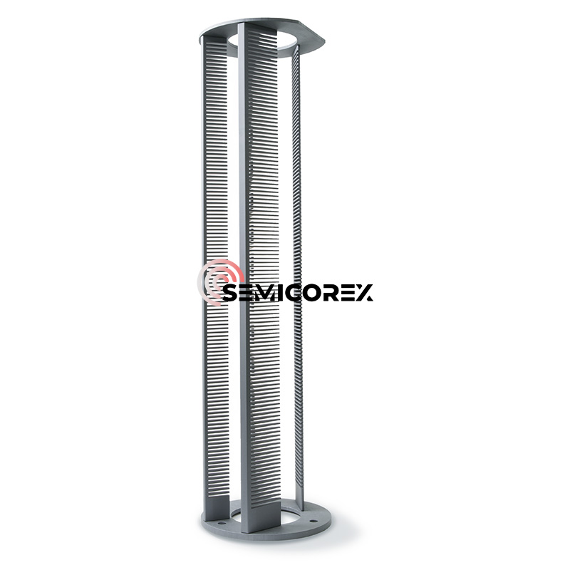
LPCVD processes, as the name suggests, operate under a reduced pressure environment, typically in the range of a few hundred to a few thousand Pascals. This lower pressure regime minimizes gas-phase collisions and scattering, resulting in improved deposition rates and enhanced film uniformity compared to atmospheric pressure CVD (APCVD). LPCVD typically requires elevated temperatures, often between 500-800°C, to drive the chemical reactions and promote film growth. Furthermore, LPCVD is often implemented as a batch process, allowing for the simultaneous processing of multiple wafers within a single reaction chamber. The batch capacity is dictated by the reactor’s design and size, accommodating anywhere from 25 to 100 or more wafers per run.

Atmospheric Pressure Chemical Vapor Deposition (APCVD)
In contrast to LPCVD, APCVD processes occur at atmospheric pressure. This simplification eliminates the need for complex vacuum systems, rendering APCVD inherently simpler and more cost-effective. However, the increased frequency of gas-phase collisions inherent to atmospheric pressure operation can negatively impact film uniformity. APCVD typically relies on higher temperatures, often reaching several hundred to a thousand degrees Celsius, to facilitate the deposition process. While APCVD may not achieve the same level of precision and uniformity as LPCVD or other advanced CVD techniques, it remains a viable option for applications where these factors are less critical. For instance, APCVD finds common use in depositing silicate glasses, such as phosphosilicate glass (PSG), and polysilicon.

Metal-Organic Chemical Vapor Deposition (MOCVD)
MOCVD stands out as a widely employed deposition technique in semiconductor manufacturing, particularly for the fabrication of compound semiconductor materials. This technique excels in the deposition of III-V semiconductors, including gallium nitride (GaN), aluminum phosphide (AlP), indium phosphide (InP), and gallium arsenide (GaAs), among others. MOCVD distinguishes itself through the use of metal-organic compounds as precursors. These compounds decompose within the reaction chamber, releasing metal atoms that subsequently deposit onto the substrate, forming the desired thin film.

Atomic Layer Deposition (ALD)
ALD operates on the principle of self-limiting surface reactions. In this process, precursor molecules react with chemically active sites on the substrate surface, forming a uniform monolayer of atoms. Once all available surface sites are consumed, the reaction ceases, hence the term “self-limiting.” This unique characteristic ensures that each ALD cycle deposits precisely one atomic layer, regardless of precursor concentration or reaction time. Consequently, ALD excels in producing thin films with exceptional uniformity, low defect density, and superior interface quality. These attributes make ALD particularly well-suited for applications demanding high-quality thin films, such as gate dielectrics in semiconductor devices and ultra-thin silicon dioxide layers.**

We at Semicorex specialize in SiC/TaC coated graphite products and CVD SiC technology applied in the MOCVD system, if you have any inquiries or need additional details, please don't hesitate to get in touch with us.
Contact phone: +86-13567891907
Email: sales@semicorex.com
Why Are Wafers Getting Larger?
Common Epitaxy Techniques and Their Characteristics: A Brief Overview
Related Article