Detailed Silicon Wafer Semiconductor Manufacturing Process
2024-11-21
How is the Process of Silicon Ingot Growth Initiated?
The process begins by placing polysilicon and dopants into a quartz crucible within a monocrystalline furnace, where the temperature is elevated to over 1000 degrees Celsius to achieve a molten state of polysilicon.

What is the Process of Monocrystal Growth?
Silicon ingot growth involves transforming polysilicon into monocrystalline silicon. After melting the polysilicon, the thermal environment is precisely controlled to cultivate high-quality single crystals.

How Are Monocrystals Formed?
Once the temperature of the polysilicon solution stabilizes, a seed crystal is slowly lowered into the silicon melt (where it also melts). The seed crystal is then gently pulled upwards to initiate crystal growth. A necking technique is employed to eliminate dislocations formed during the process. Once necking reaches a sufficient length, the crystal diameter is increased to the target dimension by adjusting the pull rate and temperature, followed by maintaining a constant diameter growth to the desired length. Finally, to prevent the reformation of dislocations, a finishing process is applied to the ingot, resulting in a completed monocrystalline ingot, which is extracted after cooling.
What Are the Methods for Preparing Monocrystalline Silicon?
The two main methods are the Czochralski (CZ) method and the Floating Zone (FZ) method. The CZ method involves melting polysilicon placed in a high-purity quartz crucible using graphite resistance heating within a cylindrical thermal system. A seed crystal is inserted into the melt surface, fused, and then rotated, while the crucible is counter-rotated. The seed crystal is gradually lifted upward through processes of crystal growth initiation, enlargement, shoulder turning, constant diameter growth, and finishing to produce monocrystalline silicon.
The FZ method involves creating a molten zone at one end of a semiconductor rod and subsequently crystallizing this zone. A single-crystal seed is fused to the molten zone, and as the temperature is adjusted, the molten zone slowly moves along the rod, turning the entire rod into a monocrystal with the same orientation as the seed. There are two types of FZ method: horizontal and vertical floating zone techniques. The former is principally used for purifying and growing single crystals of materials like germanium and GaAs, while the latter, conducted in an atmosphere or vacuum furnace, uses a high-frequency coil to create a molten zone at the contact point between the seed crystal and a hanging polysilicon rod, with the molten zone moving upwards for monocrystal growth.
What Are the Applications of CZ and FZ Methods?
Approximately 85% of silicon wafers are produced via the CZ method, and 15% via the FZ method. By application, CZ-grown monocrystalline silicon is primarily used for integrated circuit components, while FZ-grown monocrystalline silicon is used for power semiconductors. The CZ method is mature and facilitates the growth of large-diameter monocrystalline silicon; the FZ method, offering higher purity and less contamination due to the melt not contacting a container, is suitable for high-power electronic devices but struggles with producing large-diameter monocrystals, generally limited to 8 inches or less.

How is Diameter Control Achieved in Silicon Ingots?
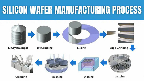
Controlling the diameter of silicon ingot rods during crystal pulling is challenging. Therefore, to achieve standard diameters like 6 inches, 8 inches, or 12 inches, the ingot diameter is ground post-pulling. This grinding results in a smooth surface with minimal dimensional error.

What Techniques Are Used for Slicing and Edging Silicon Wafers?
Using advanced wire slicing techniques, monocrystalline rods are cut into wafers of appropriate thickness. The slicing leaves wafer edges extremely sharp due to their minimal thickness, so an edging process is used to smooth the edges and reduce the risk of chipping during chip manufacturing.

How Are Wafer Surfaces Processed and Cleaned?
Lapping: This step involves placing wafers between heavy upper and lower rotating plates, applying pressure and abrasive to flatten the wafers.

Etching: This process removes surface damage by dissolving the damaged layer caused by physical processing with a chemical solution.

Double-Sided Grinding: Enhances wafer flatness by removing minor surface protrusions.

Rapid Thermal Processing (RTP): A quick heating process that stabilizes point defects within the wafer, suppresses metal impurities, and prevents semiconductor malfunctions.

Polishing: Ensures surface smoothness through precise surface processing. Using polishing slurry and cloth, combined with appropriate temperature, pressure, and rotation speed, this step eliminates the mechanical damage layer from earlier processes, achieving excellent surface flatness.

Cleaning: Removes organic residues, particles, and metals left on the wafer surface after polishing, ensuring cleanliness for subsequent processes to meet quality standards.

How Are Wafers Tested for Quality?
Flatness & Resistivity Testing: Measures parameters such as thickness, flatness, local flatness, bow, warp, and resistivity to ensure they meet customer requirements.

Particle Counting: A precise inspection step that uses laser scattering to detect surface defects and quantify them.

What is Epitaxial Growth?
Epitaxial growth involves depositing a high-quality monocrystalline silicon film on polished wafers using chemical vapor deposition. This process began in the late 1950s to early 1960s to produce high-frequency, high-power devices. It involves growing a high-resistance epitaxial layer on a low-resistance substrate, which can differ in conductivity type, resistivity, and thickness from the substrate, significantly enhancing device design flexibility and performance.

How is the Final Product Packaged?
The final stage involves packaging the qualified products to ensure their integrity and readiness for shipping.
Selective Deposition Technology
Exploring the Growth Trends in Tantalum Carbide Coating Market
Related Article
Chip processing requires numerous steps, including wafer cleaning, thermal oxidation, thin film deposition, photolithography, etching, ion implantation, annealing, diffusion, chemical mechanical polishing, and testing, ultimately resulting in a specific integrated circuit structure on the wafer.
Silicon Components in Heat Treatment
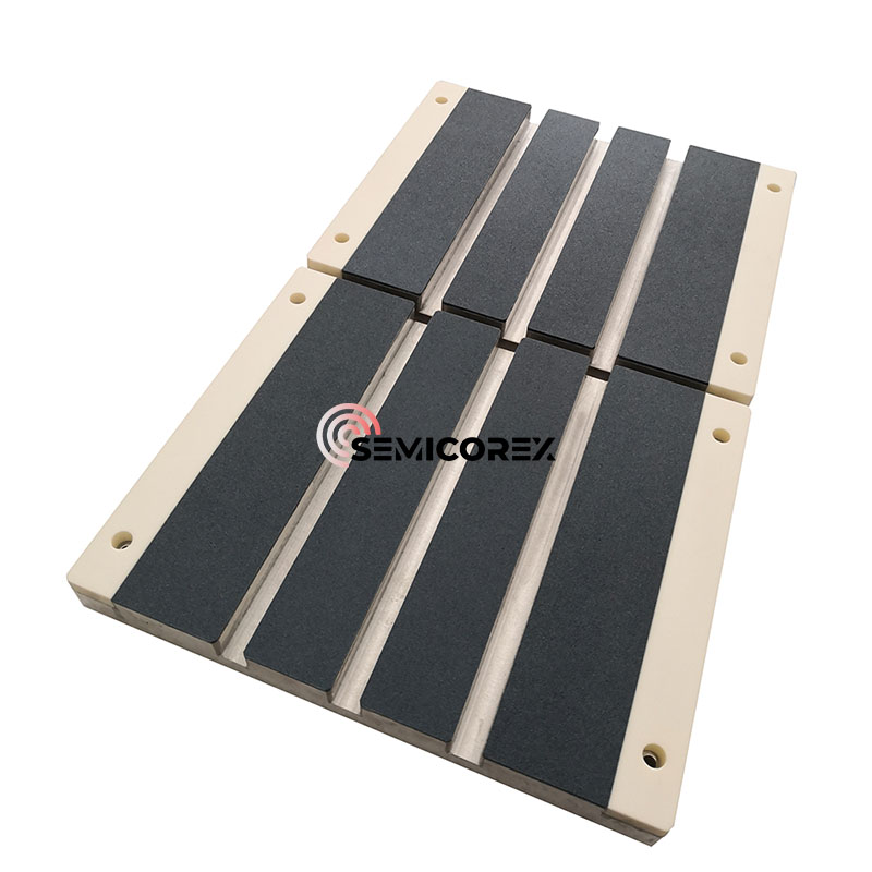
In recent years, with the continuous improvement of the performance and output of chip/thin-film electronic components such as solar cells, light-emitting diodes, semiconductors, and liquid crystal displays, there is an increasing demand for vacuum suction cups for component clamping that provide higher precision and performance.
Porous ceramic vacuum chucks