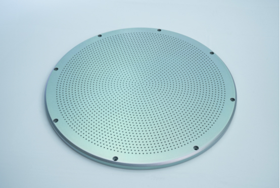
Ceramic Electrostatic Chuck: The Backbone of Secure Wafer Handling in Semiconductor Manufacturing
1. Evolving Wafer Holding Solutions
-
Mechanical Clamping: Early wafer handling relied on mechanical clamps, but their inherent limitations, including edge damage and wafer bowing, rendered them unsuitable for high-precision processes.
-
Wax Bonding: This method, while offering some improvements, suffers from low efficiency, potential contamination risks, and difficulties in achieving uniform, void-free bonding layers.
-
Vacuum Chucks: While widely used in precision grinding, vacuum chucks face limitations due to wafer deformation caused by pressure differentials and their inability to function in vacuum processing environments.
-
Electrostatic Chucks: ESCs have revolutionized wafer holding by utilizing electrostatic forces for secure, uniform, and damage-free adhesion. Their compatibility with vacuum environments and minimal contamination risks make them ideal for critical
2. Dominance of Ceramic Materials in ESCs
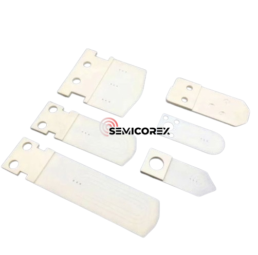
ESCs, primarily categorized by their material composition and electrostatic mechanism, utilize either alumina (Al2O3) or aluminum nitride (AlN) as the core material. Ceramic materials offer a unique combination of high thermal conductivity, wear resistance, electrical insulation, and hardness, making them superior to traditional metal or polymer alternatives.
Alumina reigns supreme as the most common ESC material, boasting superior electrical insulation compared to metals and superior wear resistance compared to polymers like PU. High-purity alumina minimizes metallic contamination, offering exceptional durability in harsh environments involving halogen gases and plasma.

Large-scale alumina ESCs utilize specialized powder formulations for uniform shrinkage, strong metal adhesion, and ease of machining. Furthermore, innovative techniques like ionic nano-coating provide cost-effective, durable insulation layers surpassing the performance of conventional co-fired alternatives.
While alumina suffices for standard silicon wafer processing, the superior thermal conductivity of aluminum nitride proves crucial for handling emerging materials like silicon carbide (SiC). Maintaining uniform wafer temperature is paramount for consistent, high-precision processing.

AlN ESCs, with their tunable electrical resistivity, provide a wide operating temperature range and sufficient holding force. Their monolithic construction through co-firing eliminates degradation issues associated with separate electrodes, ensuring consistent quality and performance. AlN’s resilience in harsh plasma and halogen environments, coupled with its stable adhesion and temperature control capabilities, makes it an ideal choice for demanding semiconductor fabrication processes.
Semicorex operates as an experienced Alumina (Al2O3)/Aluminum Nitride (AIN) ceramics manufacturer and supplier. If you have any inquiries or need additional details, please don't hesitate to get in touch with us.
Contact phone: +86-13567891907
Email: sales@semicorex.com
Plasma Etching: A Comprehensive Overview
Related Article