Common Epitaxy Techniques and Their Characteristics: A Brief Overview
-
What is Epitaxy?
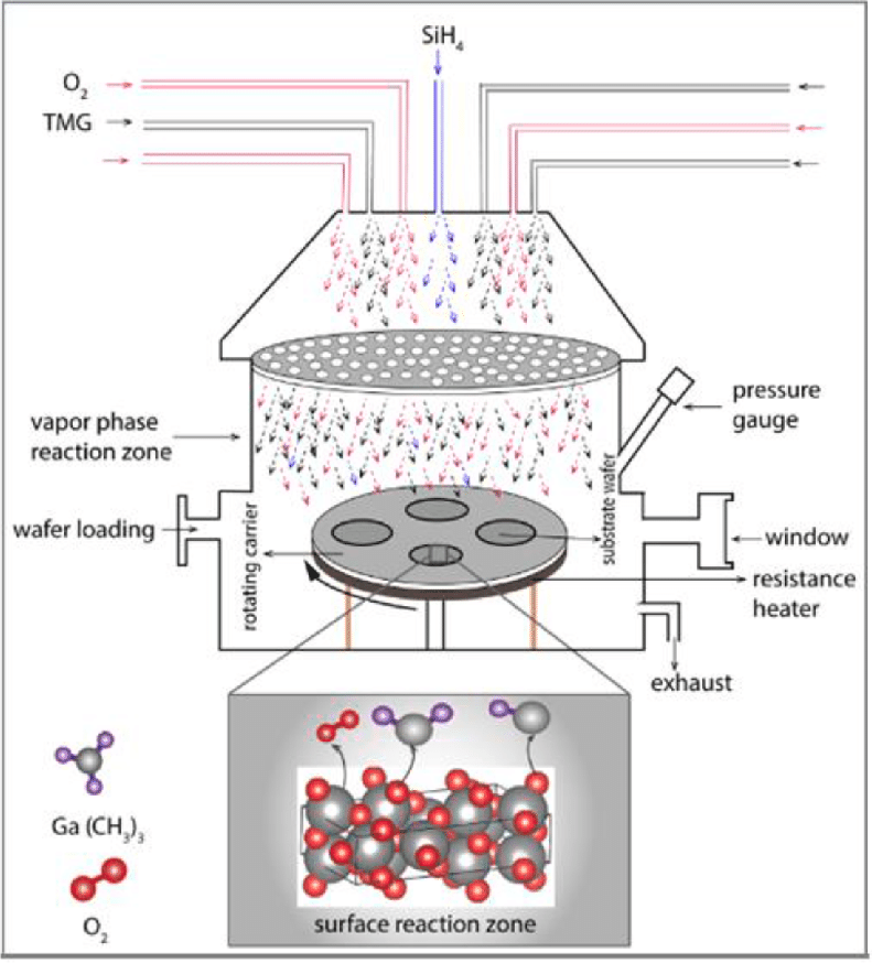
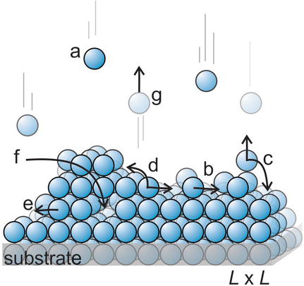
Epitaxy, derived from the Greek words "epi" (meaning "upon") and "taxis" (meaning "arrangement"), refers to the process of growing a thin, single-crystal layer on top of a single-crystal substrate. This newly deposited layer is known as the epitaxial layer.
There are 2 main types of epitaxy:
-
Homoepitaxy: Growth of the same material on a substrate of the same material. In this case, the epitaxial layer and the substrate have identical crystal structures.
-
Heteroepitaxy: Growth of a different material on a substrate of a different material. Here, the crystal structure of the epitaxial layer may differ from that of the substrate.
-
-
Single Crystal vs. Polycrystalline
-
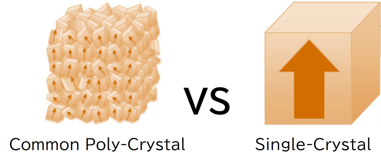
Single crystal: A material with a continuous and unchanging lattice structure throughout its entire volume. There are no grain boundaries, and the crystal orientation is uniform.
-
Polycrystalline: A material composed of many small single crystals, called grains, with different orientations. These grains are separated by grain boundaries.
While polycrystalline materials are cheaper to produce than single crystals, they are less desirable for certain applications.
-
-
Applications of Epitaxy
Epitaxy finds widespread use in various fields, including:
-
Silicon-based integrated circuit manufacturing: Silicon epitaxy is crucial for growing pure and precisely controlled silicon layers on silicon substrates, enabling the fabrication of advanced integrated circuits.
-
Power devices: SiC and GaN, two widely used wide-bandgap semiconductor materials with excellent power handling capabilities, are often grown epitaxially on silicon or other substrates.
-
Quantum communication: Superconducting qubits for quantum communication often utilize silicon-germanium epitaxial structures.
-
-
Epitaxial Growth Methods
3 commonly used epitaxial growth methods for semiconductors include:
-
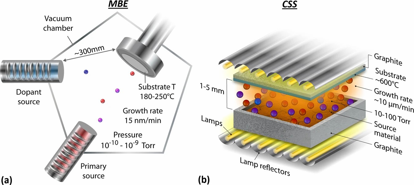
Molecular Beam Epitaxy (MBE): Conducted in an ultra-high vacuum environment, MBE involves the evaporation of source materials as atomic or molecular beams, which then deposit and crystallize onto a heated substrate. MBE offers exceptional precision and control over the deposited material thickness at the atomic level.
-
-
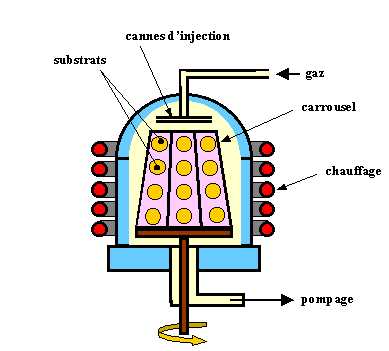
Metalorganic Chemical Vapor Deposition (MOCVD): In MOCVD, organometallic precursors and hydride gases containing the desired elements are supplied to the substrate at elevated temperatures. Chemical reactions occur, leading to the formation and deposition of the desired semiconductor material on the substrate, while byproducts are removed.
-
-
Vapor Phase Epitaxy (VPE): A crucial technique for producing semiconductor devices, VPE involves transporting vapors of elements or compounds in a carrier gas. Chemical reactions occur on the heated substrate surface, leading to the deposition of a crystalline layer.**
-
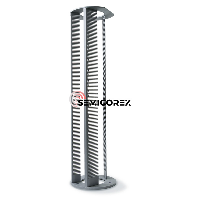
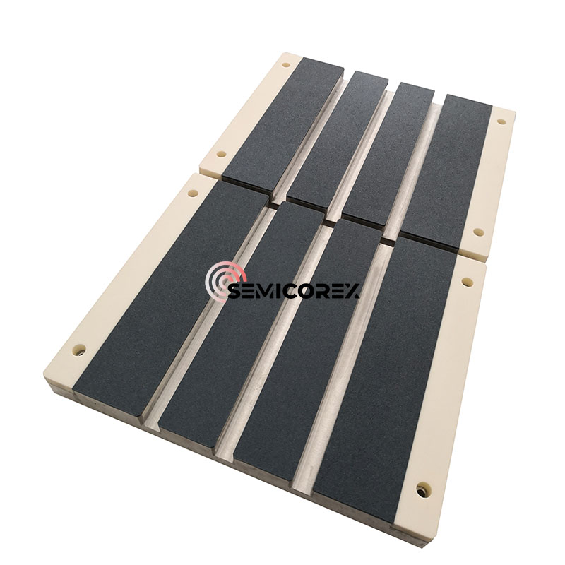
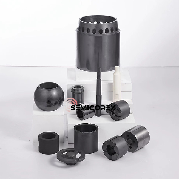
We at Semicorex specialize in SiC/TaC coated graphite products and CVD SiC technology, our offerings cater to various semiconductor applications, including integrated circuit silicon epitaxy, LED GaN epitaxy, and third-generation semiconductor SiC epitaxy.
If you have any inquiries or need additional details, please don't hesitate to get in touch with us.
Contact phone: +86-13567891907
Email: sales@semicorex.com
Chemical Vapor Deposition Techniques for Semiconductor Fabrication
Related Article