Plasma Etching: A Comprehensive Overview
Plasma etching is a critical semiconductor manufacturing process that utilizes plasma to remove or selectively etch materials from a substrate surface. It operates through a two-step mechanism:
1. Plasma Generation and Chemical Reaction: The interaction of a source gas with plasma generates chemically reactive species. 2. Surface Modification: These reactive species interact with the substrate surface, leading to the removal of targeted material.

Plasma etching offers several advantages over alternative etching techniques, establishing it as a versatile tool for high-precision pattern transfer on a wide range of materials:
-
High Speed and Cleanliness: The process is relatively fast, clean, and operates under dry conditions.
-
Material Compatibility: It exhibits compatibility with a broad spectrum of substrate materials.
-
Precision Patterning: Plasma etching enables high-fidelity pattern transfer with exceptional accuracy.
-
Etching Rate Control: The etching rate can be precisely controlled, allowing for fine-tuning of the process.
-
Enhanced Selectivity: The process offers superior selectivity, enabling the etching of specific materials while leaving others untouched.
Plasma Etching Systems and Techniques
Most plasma etching systems comprise a radio-frequency (RF) plasma source operating at 13.56 MHz, utilizing either capacitive or inductive coupling configurations. The substrate is positioned on a grounded or biased electrode. Three prominent plasma etching techniques are:
1. Reactive Ion Etching (RIE)
RIE is a widely employed plasma etching technique that utilizes chemically reactive gases to generate reactive radicals and ions. Energetic ions, accelerated by an electric field, bombard the material being etched, enhancing surface reactivity and accelerating the reaction rate with the etchant species. This synergistic interplay between chemical and physical etching mechanisms grants RIE distinct advantages over purely chemical dry etching methods.

2. Inductively Coupled Plasma Etching (ICP)
ICP etching involves placing one or more RF-powered coils around or on the reaction chamber. The alternating magnetic field generated by the RF current in the coils penetrates the chamber through a dielectric window, accelerating electrons and generating plasma. In this configuration, the coil acts as the primary inductor and the plasma as the secondary inductor. An additional RF power source connected to the substrate chuck provides bias power to control ion bombardment energy. This decoupling of ion density (controlled by coil power) and ion energy (controlled by bias power) allows for independent control over both parameters.

3. Atomic Layer Etching (ALE)
ALE is a relatively recent advancement in plasma etching technology, enabling precise material removal with atomic-level precision (approximately 0.4 nm). This technique requires a highly controlled and uniform etching process, removing material layer-by-layer with precise spatial and temporal control, resulting in exceptionally high selectivity. ALE overcomes the limitations of conventional techniques in fabricating nanoscale features, offering significant potential for future device fabrication.
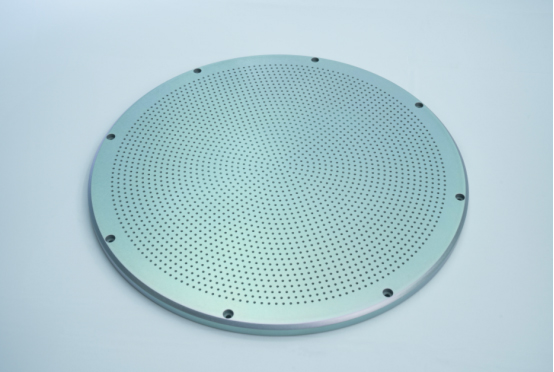
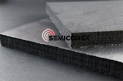
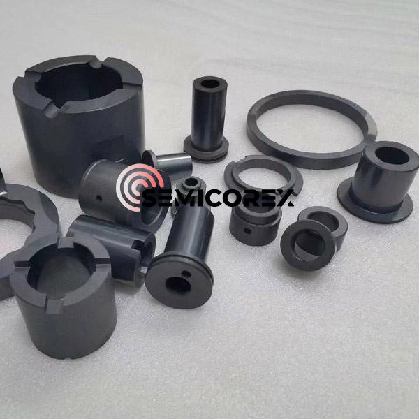
We at Semicorex specialize in SiC/TaC coated graphite products and CVD SiC technology applied in the Plasma Etching, if you have any inquiries or need additional details, please don't hesitate to get in touch with us.
Contact phone: +86-13567891907
Email: sales@semicorex.com
Isostatic Graphite: A High-Performance Material for Demanding Applications
Ceramic Electrostatic Chuck: The Backbone of Secure Wafer Handling in Semiconductor Manufacturing
Related Article