SiC Crystal Structure and Defect Control
2025-01-06
The control of crystal structure and defect management in SiC substrates are critical factors influencing their performance and applications. This article delves into the control of SiC crystal structure, defect management, and electrical property regulation, aiming to provide theoretical and practical guidance for the preparation of high-quality SiC materials.
How Does Doping Affect Lattice Hardness?
Applications of Doping in Metallurgy and Semiconductors
Doping is a common technique that involves adding impurity atoms to a lattice to adjust material properties. In metallurgy, doping is used to hinder defect movement, thereby hardening the material. In semiconductor materials, such as Gallium Arsenide (GaAs), doping specific elements can alter the dislocation behavior on different slip planes. These applications demonstrate that doping can effectively regulate the mechanical properties of crystals, providing a theoretical basis for the mechanical property control of SiC.
Doping Effects in Silicon Carbide
SiC has six main slip systems, with basal plane slip being the most common due to its lower energy requirement. However, when SiC is doped with acceptor elements like Boron (B) or Aluminum (Al), or donor elements like Nitrogen (N), the behavior of these slip systems changes. Specifically, the size difference between dopant atoms and lattice atoms generates stress in the lattice, affecting dislocation movement and slip behavior.

Position and Stress of Dopant Atoms in the Lattice
Research indicates that aluminum and boron occupy silicon and carbon sites in the SiC crystal, respectively, while nitrogen occupies carbon sites. Aluminum atoms, due to their larger radius, produce compressive stress at silicon sites; boron atoms, with a smaller radius, produce tensile stress at carbon sites; nitrogen atoms also exhibit unique stress characteristics at carbon sites. These stress differences significantly impact dislocation slip in the lattice.
How Does Doping Hinder Dislocation Slip?
The stress generated by aluminum and boron atoms in the lattice can effectively prevent basal plane slip, thereby enhancing the hardness and mechanical stability of SiC. This means that in P-type doped SiC, the formation and slip of basal plane dislocations are more hindered; in contrast, N-type doped SiC is more prone to basal plane dislocations. Therefore, by selecting appropriate dopants and doping concentrations, the mechanical properties of SiC can be precisely controlled.
How Can the Crystal Structure of Silicon Carbide Be Controlled?
Crystal Structures and Forms of Silicon Carbide
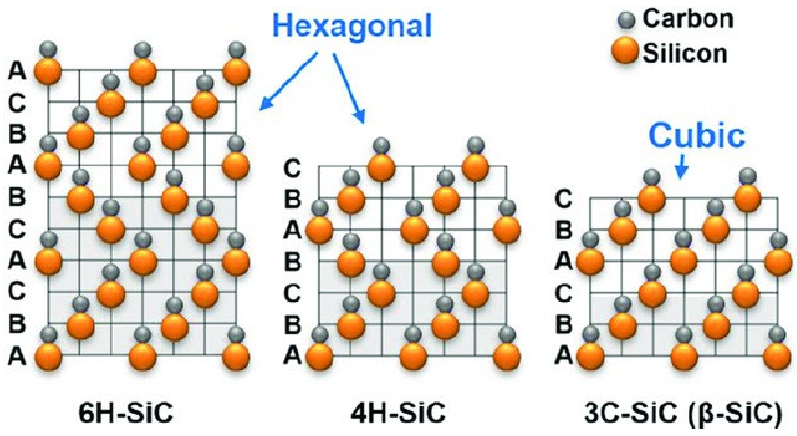
SiC exists in various crystal structures, including 3C (cubic), 4H, 6H, and 15R. The differences among these structures mainly lie in the arrangement of Si-C units in the hexagonal bilayers, which determine the crystal structure and physical properties of SiC. Additionally, the (0001) plane of SiC can be terminated with either carbon or silicon layers, depending on the type of terminating atom.
Issues with Crystal Form Inclusions
During the growth of SiC substrates, crystal form inclusions pose a significant challenge. These inclusions not only limit the growth diameter of single-crystal SiC substrates but can also act as nucleation sites for other defects, leading to a decline in crystal quality. The formation of crystal form inclusions is primarily due to their low stacking fault energy, necessitating strict control of thermal and dynamic conditions during the growth process.
Factors Influencing Crystal Form Inclusions
The formation of crystal form inclusions is influenced by several factors, including:
-
Thermal conditions and growth pressure: Precise control of temperature and pressure during the growth process is key to reducing crystal form inclusions. This requires optimization of the growth chamber design and seed crystal installation methods.
-
Surface polarity of the seed crystal: Different crystal faces have varying surface energies, leading to preferential growth of the 4H form on carbon faces with lower surface energy, and the 6H form on silicon faces with higher surface energy.
-
Gas supersaturation: Supersaturation is a crucial parameter affecting crystal form transformation. High supersaturation and specific Si/C vapor ratios are essential for the formation of the 4H form.
-
Chemical stoichiometry of the gas phase: The Si/C ratio directly affects the stability and growth conditions of the crystal form.
-
Impurity levels: Impurities in the raw materials, such as rare earth elements and nitrogen, can affect the stability of the crystal form by altering the carbon enrichment in the gas phase or changing the surface energy of the atomic nuclei.
How Are Crystal Forms Related to Growth Conditions?
The nucleation and growth temperatures of different SiC crystal forms are closely related. For example, 3C-SiC is suitable for growth at lower temperatures, while hexagonal forms require higher growth temperatures. However, due to the small energy differences between different crystal forms, precise control of crystal form transformation is challenging with temperature alone. Therefore, a comprehensive consideration of supersaturation, Si/C ratio, temperature gradient, and growth chamber pressure is necessary to effectively control the stability and transformation of crystal forms.
How Can Substrate Defects Be Managed?
Impact of Substrate Defects
Substrate defects have a highly detrimental effect on the performance of SiC devices. These defects often extend into subsequent epitaxial layers, leading to performance degradation or even device failure. Therefore, reducing substrate defects is one of the most critical challenges faced by SiC substrate technology.
Spiral Growth in Physical Vapor Transport
Physical Vapor Transport (PVT) is one of the main methods for growing SiC substrates. During the PVT process, spiral growth is a significant characteristic. Spiral growth is related to various growth factors, such as instability in growth parameters and the quality of the seed crystal. These factors can lead to two-dimensional and three-dimensional nucleation, resulting in spiral growth. Spiral growth is closely associated with the formation of crystal defects, including dislocations, crystal mosaics (domain structures), and micropipe defects.
Formation and Impact of Micropipe Defects
Micropipe defects are considered a major threat to the commercialization of SiC as a semiconductor material. These defects are large spiral dislocation hollow cores that run through the entire crystal along the growth direction, especially under conditions parallel to the c-axis. Micropipe defects can be replicated into the epitaxial layers of devices, severely impairing device performance. The formation of micropipe defects is primarily based on the Frank theory, which suggests that they form on spiral dislocations with large Burgers vectors.
Possible Sources of Micropipe Defect Formation
The formation of micropipe defects involves several aspects, including:
-
Thermodynamic sources: Uniformity of the thermal field, gas phase composition, vacancy supersaturation state, dislocation formation, and solid-state transformation.
-
Kinetic sources: Nucleation processes, growth morphology, non-uniform supersaturation states, and bubble capture.
-
Technical aspects: Instability in the growth process, seed crystal surface treatment, and contamination of the growth system.
Progress in Micropipe Defect Control
With in-depth research into the formation mechanisms of micropipe defects and precise modeling of the growth process, SiC growth technology has significantly improved. In recent years, steady progress has been made in reducing the density of micropipe defects. Currently, the commercial production of N-type 4H-SiC substrates with zero micropipe defects has been achieved.
Off-Axis Growth and Reverse "Repeat a-Face" Growth
Although micropipe defects are inherent issues in traditional PVT methods, crystals grown using off-axis growth methods (such as the Acheson process and Lely process) show fewer micropipe defects. This is attributed to the inhibitory effect of off-axis growth methods on the generation of micropipe defects. Based on this, SiC growth perpendicular to the c-axis has become a new research direction. Additionally, the Reverse "Repeat a-Face" (RAF) growth method, as a corrective technique for the growth process perpendicular to the c-axis, has demonstrated superior performance, providing new insights for the development of SiC substrate technology.
How Can Electrical Properties Be Regulated?
Significance of Resistivity
In the field of semiconductor materials, resistivity is one of the key indicators of material performance. For SiC, accurately controlling the content of dopants, whether intentional or unintentional, is a major challenge currently faced.
Differences in Requirements for High-Power and Microwave Devices
SiC is widely used in high-power devices, which require low-resistance substrates to reduce power loss, primarily caused by parasitic resistance and contact resistance. However, for devices and circuits operating at microwave frequencies, semi-insulating substrates are crucial because they can significantly reduce dielectric loss and minimize parasitic effects in devices. Therefore, resistivity regulation needs to be optimized according to specific application requirements.
Selection of Dopants and Doping Methods
In SiC, Nitrogen (N) is a commonly used N-type dopant, while Aluminum (Al) is the primary P-type dopant. These dopants create relatively shallow donor and acceptor levels in the SiC bandgap. Although Phosphorus (P) has a higher solubility in SiC than Nitrogen, and research has suggested using Phosphorus to replace Nitrogen as an N-type donor, the standard PVT method in industrial production still employs Nitrogen doping.
Nitrogen doping is typically achieved by incorporating nitrogen gas into the graphite pores of the growth crucible; in contrast, aluminum doping involves directly mixing aluminum into the silicon carbide raw material for P-type doping. However, this method faces the issue of continuous aluminum consumption, hindering the widespread application of P-type substrates.
Precise Control of Doping Levels
By accurately controlling surface polarity effects and growth parameters, the doping levels can be effectively managed. Currently, the market has achieved commercial production of highly doped (approximately 10^20 cm^-3) N-type 4H-SiC and 6H-SiC, as well as semi-insulating (approximately 10^14 cm^-3) 4H-SiC substrates. Specifically, the known lowest resistivities for 4H-SiC and 6H-SiC are 0.0028 Ω·cm and 0.0016 Ω·cm, respectively, while the highest known resistivity for 4H-SiC can exceed 10^5 Ω·cm. Due to its higher carrier mobility and lower anisotropy, 4H-SiC possesses key performance advantages in high-power and high-frequency device applications, leading to a market trend favoring the widespread adoption of 4H-SiC substrates.
Conclusion
Silicon carbide, as an excellent semiconductor material, has its performance and application range significantly enhanced by the control of crystal structure and defect management. This article has thoroughly explored the impact of doping on lattice hardness, methods for controlling SiC crystal structure, formation and control of substrate defects, and regulation of electrical properties. By designing rational doping schemes, optimizing crystal growth conditions, effectively controlling substrate defects, and precisely regulating electrical properties, the quality and performance of SiC substrates can be significantly improved, providing a solid foundation for their extensive application in high-power, high-frequency, and high-temperature devices. In the future, with further advancements in growth technology and in-depth theoretical research, the performance of SiC materials is expected to be further enhanced, propelling their applications in various fields to new heights.
We at Semicorex specialize in SiC/TaC coated graphite solutions applied in SiC semiconductor manufacturing, if you have any inquiries or need additional details, please don't hesitate to get in touch with us.
Contact phone: +86-13567891907
Email: sales@semicorex.com
What is Cassette
Ion Implantation: Halo Implant
Related Article
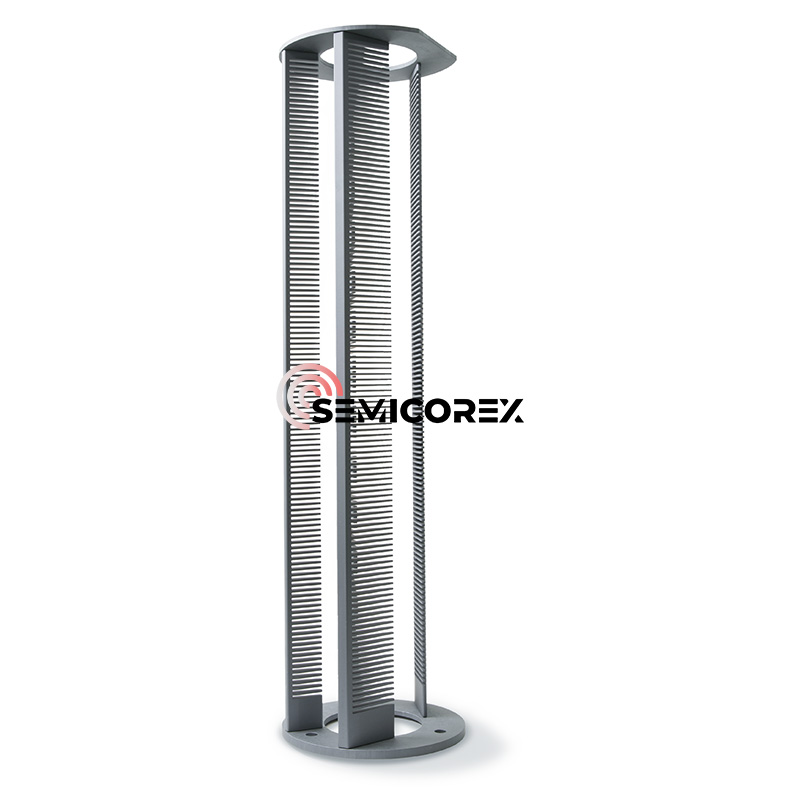
Chip processing requires numerous steps, including wafer cleaning, thermal oxidation, thin film deposition, photolithography, etching, ion implantation, annealing, diffusion, chemical mechanical polishing, and testing, ultimately resulting in a specific integrated circuit structure on the wafer.
Silicon Components in Heat Treatment
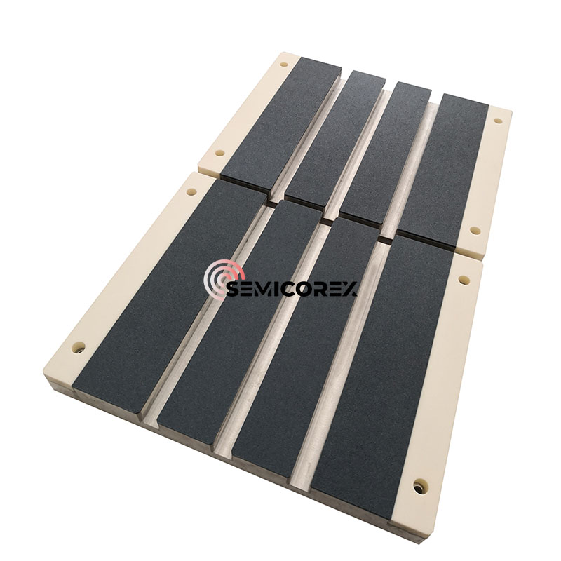
In recent years, with the continuous improvement of the performance and output of chip/thin-film electronic components such as solar cells, light-emitting diodes, semiconductors, and liquid crystal displays, there is an increasing demand for vacuum suction cups for component clamping that provide higher precision and performance.
Porous ceramic vacuum chucks