Texas Instruments Begins Production at Aizuwakamatsu GaN Factory in Japan
2024-11-01

Texas Instruments (TI) has announced the commencement of production of Gallium Nitride (GaN) power semiconductors at its plant in Aizuwakamatsu, Japan. With the Aizuwakamatsu facility operational, combined with existing GaN manufacturing operations in Dallas, Texas, TI’s in-house GaN power semiconductor capacity could quadruple.
Mohammad Yunus, TI’s Senior Vice President of Technology and Manufacturing, stated, “Leveraging over a decade of expertise in GaN chip design and manufacturing, we have successfully certified our 200mm GaN technology, which is currently the most scalable and cost-competitive method for GaN manufacturing. This milestone allows us to begin high-volume production in Aizuwakamatsu, enabling us to manufacture more GaN chips in-house and increase our internal manufacturing ratio to over 95% by 2030. We also ensure a reliable supply across our entire high-power, energy-focused GaN product portfolio by sourcing from multiple TI sites.”
TI highlighted that GaN, as an alternative to silicon, offers several advantages across various fields, including energy efficiency, switching speed, power solution size and weight, overall system cost, and performance under high-temperature and high-voltage conditions. GaN chips provide higher power density, meaning more power in smaller spaces, making them suitable for use in power adapters for laptops or mobile phones, as well as in smaller, more energy-efficient heating and air conditioning systems and household appliance motors.
Currently, TI offers the broadest range of integrated GaN power semiconductor products, covering everything from low to high voltage, enabling the creation of highly efficient, reliable, and high-power-density electronic products.
Kannan Soundarapandian, TI’s Vice President of High Voltage Power, remarked that with GaN, TI can deliver more efficient power in compact spaces, meeting a major market demand driving innovation for many of our customers. Designers of systems such as server power supplies, solar generation, and AC/DC adapters are challenged to reduce power consumption and improve energy efficiency, increasing the demand for TI’s reliable supply of high-performance GaN chips.
TI’s integrated GaN power stage product lineup allows customers to achieve higher power density, improve ease of use, and reduce system costs. Additionally, leveraging TI’s patented silicon-based GaN process, which has undergone over 80 million hours of reliability testing and includes integrated protection features, ensures the safety of high-voltage systems.
TI noted that the new capacity utilizes the most advanced equipment available today to manufacture GaN chips, enhancing product performance and process efficiency while providing cost advantages. Furthermore, TI’s continued expansion of GaN manufacturing operations incorporates more advanced and efficient tools, enabling the production of smaller chips and further packaging of additional power. This innovative design uses less water, energy, and raw materials in manufacturing, with end products using GaN chips also enjoying the same environmental benefits.
TI emphasized that scaling GaN manufacturing provides performance advantages, allowing GaN chips to operate at higher voltages, starting at 900 volts and increasing over time, driving energy efficiency and size innovation in applications such as robotics, renewable energy, and server power. Additionally, TI’s expanded investments include successful pilot operations for GaN manufacturing on 12-inch wafers earlier in 2024. TI’s continually evolving GaN process technology is fully transferable to 12-inch wafers, enabling adjustments based on customer demand and future production using 12-inch technology.**
Exploring the Growth Trends in Tantalum Carbide Coating Market
A Review of β-Ga2O3 Crystal Growth Methods
Related Article
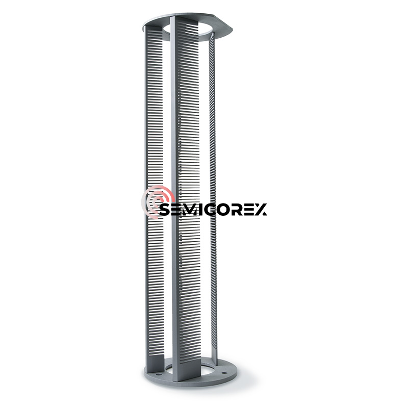
Chip processing requires numerous steps, including wafer cleaning, thermal oxidation, thin film deposition, photolithography, etching, ion implantation, annealing, diffusion, chemical mechanical polishing, and testing, ultimately resulting in a specific integrated circuit structure on the wafer.
Silicon Components in Heat Treatment
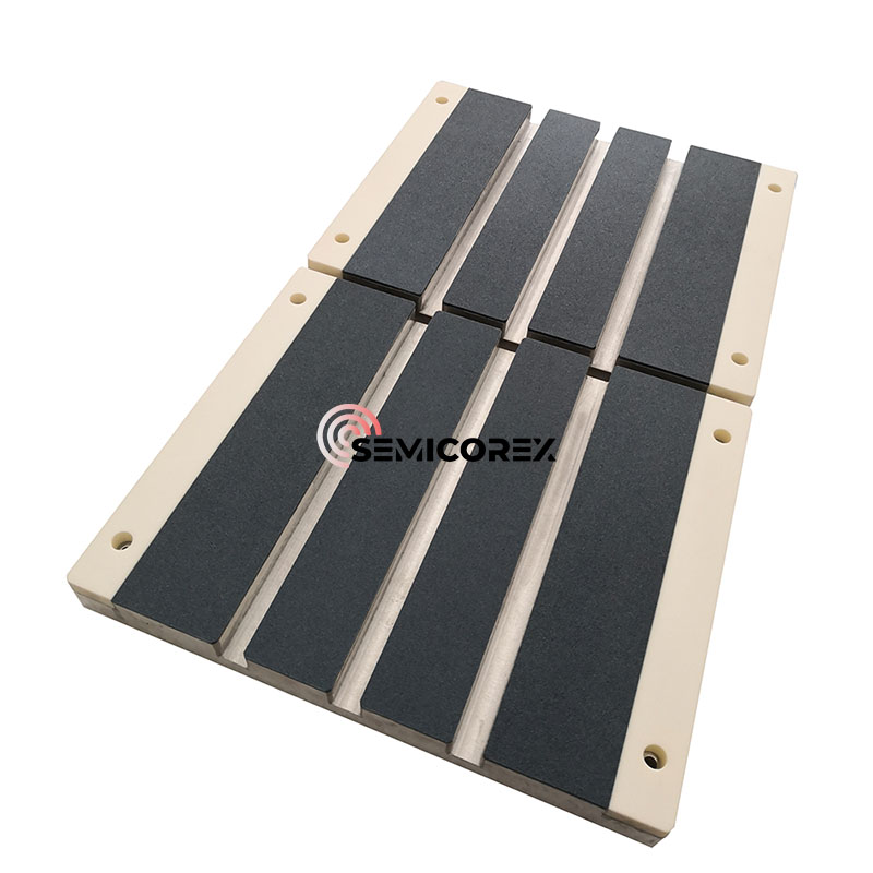
In recent years, with the continuous improvement of the performance and output of chip/thin-film electronic components such as solar cells, light-emitting diodes, semiconductors, and liquid crystal displays, there is an increasing demand for vacuum suction cups for component clamping that provide higher precision and performance.
Porous ceramic vacuum chucks