Thermal Annealing
Thermal annealing is a vital process in semiconductor manufacturing that significantly enhances the electrical and mechanical properties of silicon wafers. By exposing wafers to high temperatures, this technique effectively repairs lattice damage, activates dopants, modifies film properties, and creates metal silicides, essential for advanced semiconductor applications.

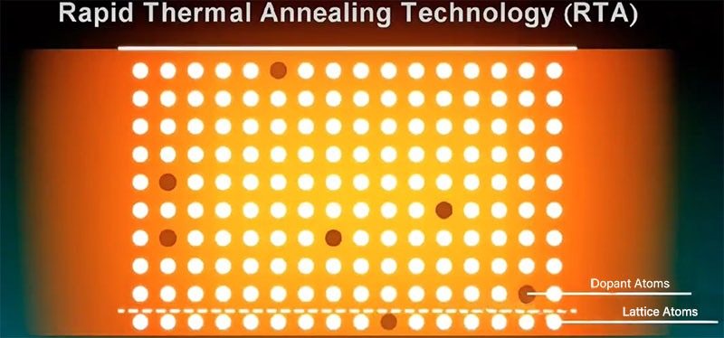
There are several types of annealing processes, each with unique features and applications. High-Temperature Furnace Annealing involves prolonged exposure to temperatures over 1000°C, making it ideal for SOI substrate preparation and deep n-well diffusion. Rapid Thermal Annealing (RTA) leverages rapid heating and cooling, completing the process in seconds at similar temperatures, crucial for forming ultra-shallow junctions in advanced node manufacturing.
Flash Lamp Annealing (FLA) and Laser Spike Annealing (LSA) represent cutting-edge methods that achieve rapid heating in milliseconds and microseconds, respectively. FLA is suited for ultra-shallow doping activation, while LSA offers high-precision control for advanced processes like FinFET and HKMG device fabrication.
In modern semiconductor manufacturing, these techniques are indispensable for various applications, including the formation of ultra-shallow junctions, modification of high-k gate dielectrics, and the formation of metal silicides. As technology nodes shrink, maintaining optimal device performance is increasingly challenging, and quick annealing technologies play a crucial role in minimizing impurity diffusion and enhancing electrical characteristics.
Ultra-Shallow Junction Formation:
Rapid thermal annealing techniques, such as RTA and FLA, ensure high impurity activation rates while minimizing impurity diffusion, catering to the demands of advanced nodes.

Modification of High-k Gate Dielectrics:
The annealing process significantly enhances the electrical properties of high-k gate dielectrics, reducing gate leakage current and improving dielectric constant, essential for advanced logic and memory devices.
Formation of Metal Silicides:
Optimizing the formation of metal silicides (e.g., CoSi, NiSi) helps lower contact resistance and body resistance, thereby enhancing device performance.
Three-Dimensional Integration Technologies:
In technologies like 3D NAND and 3D DRAM, annealing processes must be conducted across multiple layers to ensure optimal performance, with rapid annealing techniques playing a crucial role.

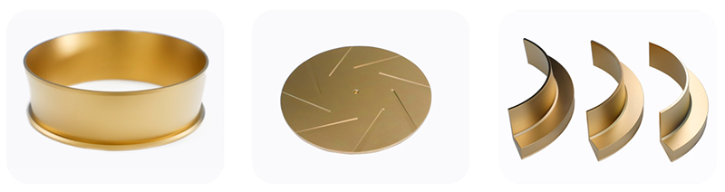
As we advance into the era of three-dimensional integration technologies such as 3D NAND and 3D DRAM, thermal annealing processes must be carefully controlled across multiple layers to ensure each layer's performance. At Semicorex, we understand the importance of tailored annealing solutions, providing customized SiC-coated parts like susceptors and covers to meet the diverse needs of semiconductor manufacturers.
By delving into the intricacies of thermal annealing, we aim to support our clients in achieving the ultimate semiconductor performance and reliability in their innovative designs.
What is FAB Process
Why Use Porous Graphite in SiC Crystal Growth?