


N-type SiC Wafer
Quantity:
N-type SiC Wafer
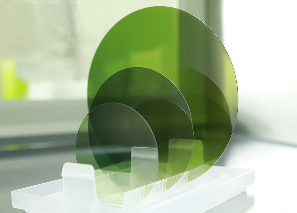
Semicorex N-type SiC wafer is a high-performance semiconductor material that offers superior electrical conductivity, thermal stability, and high-voltage tolerance, making it ideal for applications in power electronics, renewable energy systems, and optoelectronics.
Semicorex N-type SiC wafer is a high-performance semiconductor material primarily used in the development of power electronic devices, high-frequency devices, and optoelectronics. Featuring excellent electrical conductivity and thermal stability, N-type SiC wafers are ideal for applications in industries that require high power, high efficiency, and reliability under extreme conditions, such as power electronics, electric vehicles, renewable energy systems, and aerospace.
Material Properties and Structure
N-type SiC wafers are made from high-quality single crystal silicon carbide. Unlike conventional silicon wafers, which have limitations in handling high voltages and temperatures, SiC wafers provide superior performance due to their wide bandgap, high breakdown voltage, and exceptional thermal conductivity. These material properties make SiC the preferred choice for next-generation power electronics and devices that operate in extreme environments.
The N-type doping of the wafer is achieved by introducing donor elements like nitrogen or phosphorus, which provide an excess of free electrons. This doping process ensures that the wafer has an excess of electrons, making it electrically conductive. N-type SiC wafers can be used as substrates for high-power devices such as diodes, transistors, and other electronic components designed for high-voltage applications.
The structure of the N-type SiC wafer is designed to be both durable and functional, offering a smooth, polished surface with minimal defects, essential for high-performance semiconductor applications. The wafer typically comes in a variety of sizes and thicknesses to meet specific customer requirements and to fit various fabrication processes. Common diameters include 2-inch, 3-inch, 4-inch, and 6-inch, with the 4-inch and 6-inch sizes being most prevalent for large-scale power semiconductor devices.
Applications in Power Electronics
The primary application for N-type SiC wafers is in the field of power electronics. Due to their high thermal conductivity and ability to withstand higher operating temperatures, N-type SiC wafers enable the design of power devices capable of handling higher voltages and currents. These characteristics are essential in applications such as electric vehicles (EVs), where fast charging, efficient power conversion, and thermal management are critical.
N-type SiC wafers are commonly used as substrates for producing power semiconductor devices such as Schottky diodes, MOSFETs (Metal-Oxide-Semiconductor Field-Effect Transistors), and IGBTs (Insulated-Gate Bipolar Transistors). These components are integral to power conversion systems, providing efficient switching, fast recovery times, and high breakdown voltage. SiC-based devices can operate at higher temperatures than silicon-based devices, enabling more compact and reliable power electronics that require less cooling and offer higher efficiency.
The high-power characteristics of N-type SiC wafers also make them an excellent choice for renewable energy systems, including solar inverters, wind turbine control systems, and electric grid management. In these applications, SiC-based devices improve the performance and reliability of the system, enabling more efficient energy conversion and reducing overall energy loss.
Advantages of N-type SiC Wafer
High Voltage and High Temperature Performance
N-type SiC wafers are capable of withstanding high voltage and temperature conditions that would typically cause conventional silicon-based wafers to fail. This makes them highly suitable for high-power applications, including power electronics in automotive, industrial, and aerospace sectors.
Superior Thermal Conductivity
SiC has a thermal conductivity of approximately 3.7 W/cm·K, which is much higher than that of silicon. This property allows devices made from N-type SiC wafers to efficiently dissipate heat, maintaining performance and extending the operational life of the devices.
High Efficiency
Devices built using N-type SiC wafers provide higher efficiency compared to those made from silicon, due to their low on-resistance and the ability to operate at higher switching frequencies. This leads to reduced energy losses and more efficient power conversion.
Reduced Size and Weight
The high efficiency and thermal conductivity of SiC enable the design of smaller and lighter power electronic devices. This reduction in size and weight is particularly valuable in applications such as electric vehicles and aerospace, where space and weight are critical factors.
Longer Lifespan
SiC-based power devices have a longer operational life due to their robustness under high temperature and high voltage conditions. This makes them ideal for long-lasting, high-performance applications where failure is not an option.
Applications in Optoelectronics
In addition to power electronics, N-type SiC wafers are also used in optoelectronic applications, particularly in the production of light-emitting diodes (LEDs) and photonic devices. The material’s wide bandgap allows for the development of devices that operate in the UV to visible spectrum. N-type SiC wafers are commonly used in UV LEDs for sterilization, water treatment, and curing applications.
The ability to create optoelectronic devices with a high output power and efficiency in a compact form factor has made N-type SiC wafers crucial for advancing technologies in communications, sensors, and displays.
Market Trends and Future Outlook
The demand for N-type SiC wafers is projected to grow steadily over the next several years, driven by the rapid adoption of electric vehicles, the growing renewable energy sector, and increasing demand for power-efficient electronics. N-type SiC wafers are expected to play a key role in the ongoing shift towards more energy-efficient and sustainable technologies.
As more industries adopt wide-bandgap semiconductor materials like SiC, advances in manufacturing techniques and wafer production will continue to improve the quality and performance of these wafers. The ongoing development of larger diameter wafers and improved doping techniques will further enhance the scalability and cost-effectiveness of N-type SiC wafers, solidifying their position as a leading material for next-generation electronic devices.
Semicorex N-type SiC wafer is a highly versatile, high-performance material that has become indispensable in a variety of advanced technological applications. Whether for power electronics, renewable energy systems, or optoelectronics, its unique combination of superior electrical, thermal, and mechanical properties makes it the ideal choice for industries requiring reliable and efficient solutions. With continued advancements in SiC wafer technology, N-type SiC wafers are poised to play a significant role in the future of electronics, contributing to a more sustainable, efficient, and high-performance technological landscape.
Recommend Products


