


AlN Wafer Substrate
Quantity:
AlN Wafer Substrate
Semicorex AlN Wafer Substrate's properties enhances its utility in UV LEDs, UV detectors, UV lasers, and the 5G high-power/high-frequency RF devices.
One of the most prominent advantages of the AlN Wafer Substrate is its ultra-wide bandgap (Eg). Compared to first-generation silicon-based semiconductors and second- and third-generation materials like GaAs and SiC, AlN wafer exhibits a significantly wider bandgap. This ultra-wide bandgap allows the AlN Wafer Substrate to operate efficiently at higher voltages and temperatures, making it highly suitable for power electronics and high-frequency applications. The wide bandgap of AlN substrate also enables the substrate to handle more substantial electrical fields without breaking down, which is critical for devices that operate under high-stress conditions.
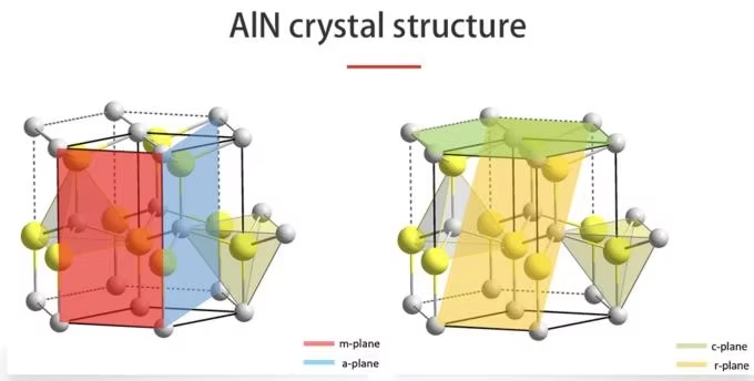
AlN Wafer Substrate Structure
In addition to its wide bandgap, the AlN Wafer Substrate boasts a high breakdown field strength (Eb). This attribute means that AlN substrate can withstand higher electric fields before becoming electrically conductive. The high breakdown field strength of AlN wafer allows devices to operate at higher voltages and power levels, which is particularly advantageous for RF and microwave applications. This property of AlN substrate also contributes to the reliability and longevity of the devices, as they are less likely to suffer from electrical breakdowns that could compromise their performance.
The thermal conductivity of the AlN Wafer Substrate is another critical advantage. Efficient heat dissipation is crucial in high-power and high-frequency applications to prevent overheating and maintain optimal performance. AlN wafer’s superior thermal conductivity ensures that heat generated during device operation is rapidly dissipated, thereby reducing thermal stress and enhancing the overall reliability of the semiconductor devices. This property of AlN substrate is especially beneficial for applications such as high-power transistors and amplifiers.
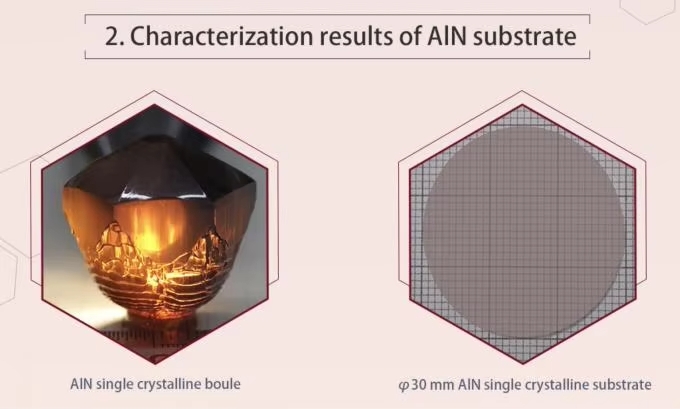
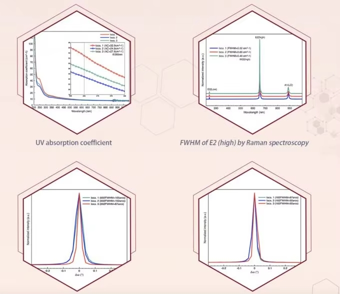
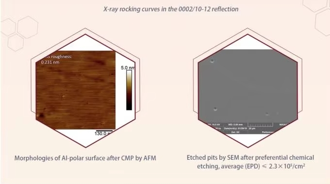
Characterization Results of AlN Substrate
In terms of material purity and quality, Semicorex’s AlN Wafer Substrates are standardized high-quality AlN substrates, available in various dimensions including 10x10mm, Φ10mm, Φ15mm, Φ20mm, Φ25.4mm, Φ30mm, and Φ50.8mm. These AlN substrates are crafted with precision to ensure consistency and reliability in semiconductor manufacturing processes.
Moreover, Semicorex also supplies non-polar M-face AlN substrates in the 10-20mm range. Non-polar substrates are particularly advantageous for certain applications where reducing polarization effects can lead to improved device performance. The availability of non-polar M-face AlN substrates provides versatile and high-performance materials to meet the diverse requirements of the semiconductor industry.
The application potential of the AlN Substrate spans several cutting-edge technologies. In the realm of ultraviolet (UV) LEDs, the wide bandgap of AlN wafer makes it an ideal substrate material. UV LEDs are used in a variety of applications including sterilization, disinfection, and water purification. The high efficiency and reliability of AlN-based UV LEDs make AlN substrate superior to traditional mercury-based UV lamps.
For UV detectors and UV lasers, the AlN Wafer Substrate provides significant performance benefits. UV detectors are essential in fields such as astronomy, environmental monitoring, and industrial process control. The high sensitivity and stability of AlN-based UV detectors ensure accurate and reliable measurements. Similarly, UV lasers, which are used in medical diagnostics, communication technologies, and advanced manufacturing, benefit from the high power handling and thermal management capabilities of AlN substrates.
In the rapidly evolving realm of 5G technology, the AlN Wafer Substrate plays a crucial role in the development of high-power/high-frequency RF devices. The exceptional thermal conductivity and high breakdown field strength of AlN substrate make it well-suited for high-frequency transistors and amplifiers that are essential components of 5G infrastructure. The use of AlN substrates in these devices ensures robust performance, reduced thermal degradation, and enhanced reliability.
Furthermore, the robustness and high-temperature stability of the AlN Wafer Substrate open up possibilities for its use in harsh environments and demanding applications. Aerospace, automotive, and industrial sectors can benefit from AlN substrate’s ability to maintain performance under extreme conditions. For instance, in aerospace applications, AlN substrates can be used in sensors and communication devices that must withstand high temperatures and radiation levels. AlN wafer’s inherent durability and reliability ensure consistent performance even in the most challenging environments.
Recommend Products

