Alumina Ceramic Robotic Arms
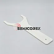
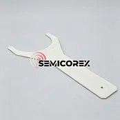
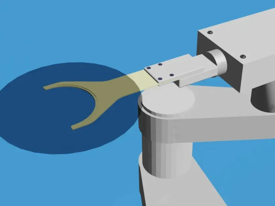
Semicorex alumina ceramic robotic arms function for high-precision wafer gripping, transfer, and positioning in wafer handling robots, vacuum transfer manipulators, and lithography machine loading systems. By using Semicorex alumina ceramic robotic arms, the risks of particle contamination and mechanical damage to semiconductor wafers can be significantly avoided, perfectly satisfying the rigorous requirements of semiconductor manufacturing.
Advantages of Semicorex alumina ceramic robotic arms
1. Reliable load-bearing capacity
Semicorex aluminaceramicroboticarms are manufactured from nano-grade alumina powder and sintered at high temperatures, allowing them to feature superior flexural strength and fracture toughness. Benefiting from such superior mechanical strength, Semicorex aluminaceramicroboticarms are capable of loading 1-15 kg weights, which effectively guarantees stable and safe wafer handling throughout semiconductor production.
2. High cleanliness performance
Semicorex alumina ceramic robotic arms feature a dense monolithic ceramic structure and can significantly avoid particle shedding and metal ion release during actual operation. Boasting dependable chemical stability, Semicorex alumina ceramic robotic arms resist strong acids, bases, and organic solvents, effectively minimizing chemical by-products generated in critical processes such as wet cleaning and chemical vapor deposition (CVD).
3. Flexible compatibility and dimensional accuracy
Semicorex offers customized services for our customer and supports customization strictly based on customer specifications and drawings, which ensures perfect compatibility with customers’ automated wafer handling equipment. Each alumina ceramic robotic arm from Semicorex features tight dimensional tolerances, enabling precise wafer alignment and positioning during cutting-edge semiconductor manufacturing.
Application scenarios
1. Semiconductor manufacturing
Aluminaceramicroboticarms can be applied to FOUP handling, wafer transfer in vacuum chambers and loading or unloading for lithography and etching machines in wafer fabrication, as well as applied in chip sorting and ultra-clean packaging lines during semiconductor packaging and testing processes.
2. Photovoltaic and electronics industry
Aluminaceramicroboticarms are also well-suited for solar wafer sorting, precision assembly of PCB boards, and automated production of MEMS sensors in the advanced photovoltaic and electronics industry.