

Focus Rings
Quantity:
Focus Rings
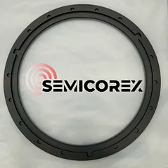
Semicorex Focus Rings are critical plasma etching component that surrounds the wafer and applies voltage to concentrate plasma, enhancing etch uniformity across the wafer surface.
Semicorex Focus Rings are critical components used in the plasma etching process within semiconductor manufacturing. Positioned around the periphery of the wafer, these specialized CVD SiC Focus Rings play a pivotal role in maintaining etch uniformity and enhancing device yield. As a direct-contact part that interfaces closely with the wafer edge, the Focus Ring is designed to control the distribution and behavior of plasma, enabling high-precision pattern transfer during the etching stage.
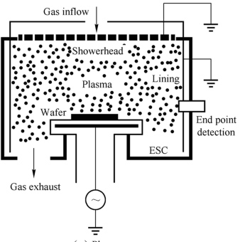
TheCVD SiC Focus Rings operate by shaping the electric field within the etching chamber. During the etching process, high-frequency RF power is applied to create a plasma field composed of reactive ions and radicals. The Focus Ring is strategically placed at the edge of the wafer, often fabricated from materials compatible with the chamber environment and resistant to plasma-induced erosion. By applying a voltage to the Focus Ring, the electric field is locally adjusted, effectively focusing the plasma closer to the wafer surface and particularly toward its edges.
This controlled focusing minimizes plasma divergence and contributes to a more uniform ion bombardment across the entire wafer surface. As a result, the cvd sic Focus Rings significantly improve etch uniformity — a key factor in producing consistent and reliable semiconductor devices, especially as wafer sizes increase and process nodes shrink.
Thecvd sic focus rings are the important component placed outside the wafer and directly in contact with the wafer. By applying voltage to the ring to focus the plasma passing through the ring, the plasma is focused on the wafer to improve the uniformity of processing.
Since the focus ring will directly contact the plasma in the vacuum reaction chamber, it is necessary to use a material that is resistant to plasma corrosion. Traditional focus rings are made of silicon or quartz. Conductive silicon is a commonly used focus ring material. Its conductivity is almost close to that of silicon wafers, but its disadvantage is that it has poor etching resistance in fluorine-containing plasma. The materials of the etching machine components often suffer from severe corrosion after a period of use, which seriously reduces its production efficiency.
Silicon carbide has similar conductivity to silicon and good ion etching resistance. With the advancement of integrated circuit miniaturization, the demand and importance of etching processes in integrated circuit manufacturing are increasing, and the power and energy of etching plasma continue to increase. In particular, the plasma energy required in capacitively coupled (CCP) plasma etching equipment is higher, so the utilization rate of focus rings made of silicon carbide materials is increasing.
Recommend Products